PCB antenna rendered useless by overly enthusiastic copper fill.

The Many Ways You Can Easily Ruin Your PCB Antenna Design

PCB antenna impaired by copper fill and other attenuation sources.

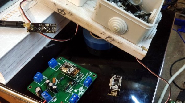
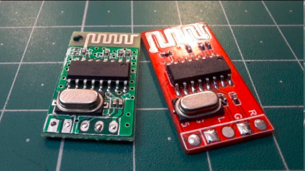
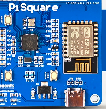
We have all seen Printed Circuit Board (PCB) antennas: those squiggly bits of traces on PCBs connected often to a Bluetooth, WiFi or other wireless communication chip. On modules like for the ESP8266 and ESP32 platforms the PCB antennas are often integrated onto the module’s PCB, yet even with such a ready-made module it’s possible to completely destroy the effectiveness of this antenna. These and other design issues are discussed in this article by [MisterHW].

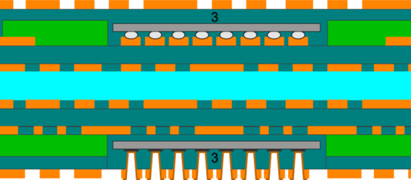
It covers a range of examples of poor design, from having ground fill underneath an antenna, to having metal near the antenna, to putting dielectric materials near or on top of the antenna. The effect of all of these issues is generally to attenuate the signal, sometimes to the point where the antenna is essentially useless.

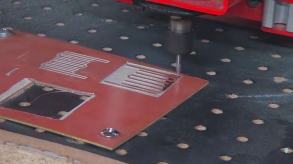
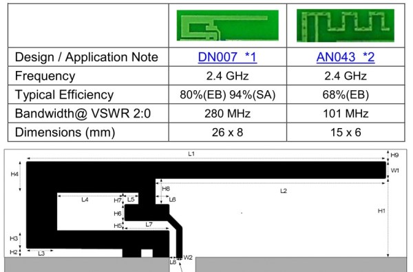
Ultimately, the best PCB antenna design is one where there is no nearby copper fill, and there are no traces running near or on layers below the antenna. After all, any metal trace or component is an antenna, and any dielectric materials will dampen the signal. Fortunately, there is e.g. a free KiCad library with ready-to-use PCB antenna designs to help one get started with a custom design, as well as many other resources, covered in the article.

If you want to get really professional about checking the effectiveness of an antenna design, you’ll want to use a Network Vector Analyzer. These will also help you with tuning the capacitors used with the PCB antenna.

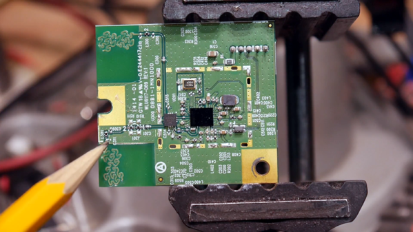
(Featured image: PCB antenna rendered useless by overly enthusiastic copper fill.)

Fixing NRF24L01+ Modules Without Going (Too) Insane

Good old nRF24L01+ wireless modules are inexpensive and effective. Well, they are as long as they work correctly, anyway. The devices themselves are mature and well-understood, but that doesn’t mean bad batches from suppliers can’t cause hair-pulling problems straight from the factory.

[nekromant] recently got a whole batch of units that simply refused to perform as they should, but not because they were counterfeits. The problem was that the antenna and PCB design had been “optimized” by the supplier to the point where the devices simply couldn’t work properly. Fortunately, [nekromant] leveraged an understanding of the problem into a way to fix them without going insane in the process. The test setup is shown in the image above, and the process is explained below. Continue reading “Fixing NRF24L01+ Modules Without Going (Too) Insane”

Bandpass Filters From The CNC Mill

A bandpass allows a certain electrical signal to pass while filtering out undesirable frequencies. In a speaker bandpass, the mid-range speaker doesn’t receive tones meant for the tweeter or woofer. Most of the time, this filtering is done with capacitors to remove low frequencies and inductors to remove high frequencies. In radio, the same concept applies except the frequencies are usually much higher. [The Thought Emporium] is concerned with signals above 300MHz and in this range, a unique type of filter becomes an option. The microstrip filter ignores the typical installation of passive components and uses the copper planes of an unetched circuit board as the elements.

A nice analogy is drawn in the video, which can also be seen after the break, where the copper shapes are compared to the music tuning forks they resemble. The elegance of these filters is their simplicity, repeatability, and reproducability. In the video, they are formed on a CNC mill but any reliable PCB manufacturing process should yield beautiful results. At the size these are made, it would be possible to fit these filters on a business card or a conference badge.

Continue reading “Bandpass Filters From The CNC Mill”

Teardown Locates Fractal Antenna

[IMSAI Guy] tore apart a device with a wireless network card and decided to investigate what was under the metal can. You can see the video of his examination below. Overall, it was fairly unremarkable, but one thing that was interesting was its use of an antenna on the PCB that uses a fractal design.

You probably know fractals are “self-similar” in that they are patterns made of smaller identical patterns. The old joke is that the B. in Benoit B. Mandelbrot (the guy who coined the term fractal) stands for Benoit B. Mandelbrot. You can think of it as akin to recursion in software. Antennas made with fractal patterns have some unusual and useful properties.

Continue reading “Teardown Locates Fractal Antenna”

The Components Are INSIDE The Circuit Board

Through-hole assembly means bending leads on components and putting the leads through holes in the circuit board, then soldering them in place, and trimming the wires. That took up too much space and assembly time and labor, so the next step was surface mount, in which components are placed on top of the circuit board and then solder paste melts and solders the parts together. This made assembly much faster and cheaper and smaller.

Now we have embedded components, where in order to save even more, the components are embedded inside the circuit board itself. While this is not yet a technology that is available (or probably even desirable) for the Hackaday community, reading about it made my “holy cow!” hairs tingle, so here’s more on a new technology that has recently reached an availability level that more and more companies are finding acceptable, and a bit on some usable design techniques for saving space and components.

Continue reading “The Components Are INSIDE The Circuit Board”

PCB Design Guidelines To Minimize RF Transmissions

There are certain design guidelines for PCBs that don’t make a lot of sense, and practices that seem excessive and unnecessary. Often these are motivated by the black magic that is RF transmission. This is either an unfortunate and unintended consequence of electronic circuits, or a magical and useful feature of them, and a lot of design time goes into reducing or removing these effects or tuning them.

You’re wondering how important this is for your projects and whether you should worry about unintentional radiated emissions. On the Baddeley scale of importance:

  • Pffffft – You’re building a one-off project that uses battery power and a single microcontroller with a few GPIO. Basically all your Arduino projects and around-the-house fun.
  • Meh – You’re building a one-off that plugs into a wall or has an intentional radio on board — a run-of-the-mill IoT thingamajig. Or you’re selling a product that is battery powered but doesn’t intentionally transmit anything.
  • Yeeeaaaaahhhhhhh – You’re selling a product that is wall powered.
  • YES – You’re selling a product that is an intentional transmitter, or has a lot of fast signals, or is manufactured in large volumes.
  • SMH – You’re the manufacturer of a neon sign that is taking out all wireless signals within a few blocks.

Continue reading “PCB Design Guidelines To Minimize RF Transmissions”

PCB Antenna Reference Designs

Have you ever built a wireless project and weren’t sure how to make one of those awesome (and cheap!) PCB antennas? “What low-cost solutions does our Antenna Board #referencedesign contain?” said Texas Instruments (TI) recently via Twitter.  This older reference design contains some comprehensive designs for sub-1 GHz and 2.4 GHz antennas.

While TI’s documentation can be difficult to navigate, there are many hidden gems, and this is one of them. While TI created these designs for use with their wireless products, they will work on any device which utilizes the same wireless base frequency. For example, you could use any of the 2.4 GHz antennas with any Bluetooth, WiFi (2.4 GHz), or Bluetooth Low Energy chips. Simply open up their Antenna Selection Quick Guide document and navigate to the specific design for whichever antenna you would like to build.

For a more detailed overview of what goes into designing and testing a PCB antenna, check out this hack which we featured back in 2010. With the internet of things coming into its own, wireless projects will become more and more prolific, making PCB antennas more important than ever.