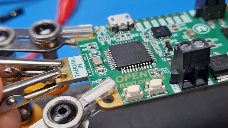
Surface mount components have been a game changer for the electronics hobbyist, but doing reflow soldering right requires some way to evenly heat the board. You might need to buy a commercial reflow oven — you can cobble one together from an old toaster oven, after all — but you still need something, because it’s not like a PCB is going to solder itself. Right?
Wrong. At least if you’re [Carl Bugeja], who came up with a clever way to make his PCBs self-soldering. The idea is to use one of the internal layers on a four-layer PCB, which would normally be devoted to a ground plane, as a built-in heating element. Rather than a broad, continuous layer of copper, [Carl] made a long, twisting trace covering the entire area of the PCB. Routing the trace around vias was a bit tricky, but in the end he managed a single trace with a resistance of about 3 ohms.
When connected to a bench power supply, the PCB actually heats up quickly and pretty evenly judging by the IR camera. The quality of the soldering seems very similar to what you’d see from a reflow oven. After soldering, the now-useless heating element is converted into a ground plane for the circuit by breaking off the terminals and soldering on a couple of zero ohm resistors to short the coil to ground.
The whole thing is pretty clever, but there’s more to the story. The circuit [Carl] chose for his first self-soldering board is actually a reflow controller. So once the first board was manually reflowed with a bench supply, it was used to control the reflow process for the rest of the boards in the batch, or any board with a built-in heating element. We expect there will be some limitations on the size of the self-soldering board, though.
We really like this idea, and we’re looking forward to seeing more from [Carl] on this.
Thanks for the tip, [Tobias].


I did not watch the video, I only read the article – but the idea behind this sounds pretty smart to me. Nice trick indeed.
And pretty out of specification!
But not good for every pcb ,,😊😊😊
With the solder paste being electrical conductor, the pre-programmed MCU could almost reflow itself until the T°juction reaches critical temperature…
Joke aside, it’s nice hack, but in real life, I don’t see the point as it increase PCB cost and reduce ground performance.
Once fused, connect the thermal plane to ground?? Maybe via thermal fuses, that connect on melting? Don’t know, not an EE.
Obv didn’t read the article, watched the vid though. Fail-closed thermal fuses would make the assembly even more automatic.Or use a *separate* ground plane as a heat spreader.
Article pretty much sums up the “real life” usage here as he needed to reflow without use a reflow oven the internally reflowed board would ultimately wind up in. I could imagine manufacturers offering these for the hobbyist like myself that will happily put components together but won’t invest in an oven
Very nicely done. We don’t use self-heating circuits enough. It would be nice to have a heating element circuit as part of nitinol shape-memory devices to allow for heating on demand to reset the nitinol shape-memory.
It would also be nice to have addressable circuit heating elements in structural alloys to be able to readjust microstructures, e.g. when you need austenite recreated.
Did you just made reballing a 1min process ?
Might make a good ground plane layer in some applications too!
As stated in the article.
Meow
Note that while it will be an OK return path for DC loads, it’ll become a high-impedance antenna under even high audio frequencies (10kHz). At high frequencies those 0ohm resistors he uses to short the coil to ground act as inductors themselves, though the problems would pale next to those caused by return path issues.
Rick Hartley did a great talk at an Altium conference on this a few years back, “How to Achieve Proper Grounding” on Youtube.
40:25-45:30 most clearly illustrates what relying on a circuitous path for ground return would do, though 22:55-36:00 really helps build the intuitive groundwork (and gives me that 10kHz number), 54:30-57:00 gives ideas for good layer stackups. The whole talk is really good.
Not that this doesn’t have its place. For hobbyist stuff under 10MHz it’ll probably fine, at least if there isn’t sensitive analog stuff going on. For a product, this could easily FCC testing issues. An easy mitigation would be putting the heating coil on the 3rd or 4th plane (if there isn’t much happening on the backside, or if you’re springing for a 6+ layer board) so the 2nd plane can be used as a proper ground plane.
Add some vias and pads that are exposed around the edges to stitch the traces together afterwards. Adds a manual post-reflow soldering step, but it means all the fiddle SMT parts ‘solder themselves’ and you just need to drag solder a single stripe across the board to turn the ‘ground zig-zag’ into a perforated ground plane.
Sounds good for a Mars rover PCB too!
That was my thought too. Built in heater for circuit boards that have to work in extremely cold environments. Include a SMT temperature sensor IC + PWM-based power control for the heater and the on-board micro could regulate the temperature.
They usually just add extra resistors that serve as heaters. A lot more flexibility that way, and works with lower layer count and through-hole designs too.
Already quite common to use ohmega ply layers as board heaters in some space applications.
The fancy HP measuring equipment had a little oven inside to control the temperature of the timebase oscillator.
Putting in a second-layer heating element under your SiTIME adjustable frequency clock so you can guarantee it’s always at 40C suddenly seems like a pretty fun modern version of this.
Use the power transistor you need to control the temperature as a heater
Imagine instead of blowing a chip as an encryption fail-safe, all of the components just fall off the board lol
It would be a royal nuisance, but if you know that could happen, you could take a hi-res picture of the board before messing with it.
Blowing a chip is final.
“Blowing a chip is final.”
Magic smoke release technology.
I’ve seen this in person with a board that was vertically oriented. A software glitch could create a situation where the power would shoot-through a push-pull driver. When this happened you could collect most of the parts in the bottom of the case.
Hey what about making alternative footprints for components (kicad maybe I dunno) so the coil for each component is included, you simply connect each other in a final step,after all why heating in places where there are no pads? you can hide the layer with coils to work in the original circuit and perhaps a plugin to make some autorouting for the coils. so what do u think folks?
You want to have the board heat up +- evenly, otherwise it might bend. Also, you need to control which layer the in-footprint coil appears on, which isn’t made easy in KiCad, and for a good reason – it isn’t something typically required.
Good point, but I remember an old video about soldering individual pads with a laser beam. Then we have those selective wave soldering machines maybe is just about try and error and adjusting the temp curves, who knows maybe it just I drank so much coffee :)
That’s brilliant. Could also be used for self-recycling to remove the components at the end of life.
My thoughts exactly, it would be really nice way to pull out that MCU for your next project. Also it could be nice if your supplier doesn’t have those in stock due to chip shortage.
Add few big 0R on top layer as part of the heating current path, then flip the board upside down and the components just fall off with automatic shutdown :P.
Planned Obsolescence.
Yes let’s not make it too easy for Apple turn our electronics in to proverbial lemons.
“That’s brilliant.”
Yeah, specially in the infrared… [runs and ducks]
I made some self heating PCBs to control the temperature of components. Used simple resistors though, not a trace.
I knew this was a Carl B project from the headline! He’s a PCB genius beyond compare.
If it can self solder, then it can self unsolder.
An interesting self destruct mechanism.
A bit more current and it can catch on fire too.
I honestly tried this before years ago. The pcb delaminated a bit and caused fractures on the traces. I gave up on it when I realized it wouldn’t be suited for RF/Audio.
Not cheap. In the video his order goes from $50 to $150 when he selects high temperature PCBs. I’m sure heating the inside instead of outside of the PCB is why this is required. I played with the PCBway calculator, the high temp PCBs double or triples the price depending on size and quantity.
If the track were a coil instead of a dumb resistor, it could also serve as a power source when placed over a QI charger, so at least you are not loosing that ground plane for nothing once it’s soldered.
I like the idea of adding wireless charging a lot. Probably get a watt or two without too much heat.
Nice…
– Test to failure without a fume extractor, and done indoors. All kinds of nasty compounds are being produced* – like (brominated) aromatic hydrocarbons.
– A lot of the excess stresses and potential delamination issues go away when the PCB heater is combined with e.g. a toaster oven or sandwich toaster that’s stabilized at 100-150°C. Then the PCB heater can contribute the fast time constant temperature control, and the PCB still has a bath temperature to settle back to. Holding the PCB at 125°C for example is a complete non-issue: 150Tg or 170Tg have this as an actual operating temperature. Don’t hold your PCB at 125°C for 2000 hours or so, but 10-30 minutes won’t do any harm. In turn, you get rid of a 100 K gradient towards the environment and retain full and fast control over the reflow process.
– Copper has alpha of 3870-3930 ppm/K, there’s nothing wrong with implementing a 4-wire temperature measurement with the Cu trace itself to extract an equivalent heater temperature, which also conveniently allows limiting the internal temperature to prevent fun destruction and fire. Too much to ask for from generation Arduino?
* https://www.researchgate.net/publication/265173656_Pollutant_emissions_during_pyrolysis_and_combustion_of_waste_printed_circuit_boards_before_and_after_metal_removal
Is anybody here thinking of the recycling potential as in a board that dismantles itself? You could have products which you plug in at end of life and they automatically desolder themselves and with a quick flick all the components are released to a tray.
As opposed to passing the board through an oven with a jiggly bed, youd bed compliant connectors and a process to connect them? Seems a bit faffy to me.
Yes, Phil Rogers, CRJAA and maybe othes already mentioned that. Did you read the comments yourself before posting?
It wouldn’t be cost effective to reclaim the components. I was thinking of the reprap project, how its goal was to assemble itself. it could solder a controller with this method.
It’s a nice trick, but I do have doubts about viability. For dissasembly it would be just silly. If that is even done, it would be done on a large scale, maybe by putting 1000’s of PCB’s through a shredder or whatever.
4-layer PCB’s are significantly more expensive than 2 layers, and this would limit it to small kits, maybe there is some room in the market for that, but even a “serious hobbyist” has some kind of reflow oven, hotplate or hot air gun these days.
Another thing I don’t agree with is using it as a GND plane. Those serpentine tracks are not a good GND plane at all, even when you do stitch them together later. On the other side, they can be used for the power distribution instead of the GND plane. That would make a lot more sense.
I would think normal FR-4 (not high-temp) would work here. After all, normal FR-4 is reflowed all the time. As long as you can meet the thermal cycle timing, then it should be ok. I don’t think it would matter if heat comes from inside or outside, but more work could be done here to improve the thermal profile.
The reflow oven profile is maybe three minutes long. The FR4 never gets anywhere near this hot. I do “high temperature” testing of components all the time and even at 125C the soldermask starts discoloring and the board life is shorter. If you heat the inner layers of FR4 up enough to get the surface to reflow temperatures, you’re going to cook your PCB. I suspect the epoxy used in laminating the layers will start failing, among other things.
You are right regardinmg reflow. But If PCBs get problems already at 125°C stronmgly deopends on material. In the last years at work I did many products, which had to (and did) reliably work at 125°C. (85 ambient plus self heating of all the power MOSFETs
If you did this with a general purpose prototyping style board, lay down a few standard IC footprints and traces to test points, and some areas with grids of uncommitted pads, it could become an interesting and reuseable lab resource. Plus your prototype could be used in real life, as opposed to a plug-in board where things can fall out.
Indeed.
Or just a breakout board.
A person can fit a bunch of common footprints onto a 2-sided PCB with rows of pin headers that connect to them.
If the boards could be made cheap enough (which is probably just a matter of quantity), and there were maybe even reusable stencils that could also be purchased, then this might be a boon for prototyping with modern SMT ICs.
It might not be the best thing for production, for all of the RFI and ground plane issues mentioned by others, but…
I, for one, would pay a love to have a stack of universal-ish breakout boards that can be reliably self-soldered.
From an RF immunity / emissions stand point, slots in a ground plane are generally a very bad idea. That’s a great way to make an antenna that you don’t want.
Also, on boards with more than a few 10s of mA loads this means that you are going to end up with higher voltage drops along the ground path than a uninterrupted plane would.
if only the xbox 360 had that
I love it! Great idea. I may also reduce manufacturing environmental impacts!
Unfortunately not. Extra circuitry (and a bad ground palne) in every device. Better to have one dedicated reflow oven.
Circuit boards soldering other circuit boards? Do you want a machine uprising? …because this is how it starts.
Still – pretty ingenious. Great idea. love it.
I thought this was just a cool idea when I first read this. But when I was posting a Slashdot comment about the same story, I realized there are some potentially very practical benefits that might offset the drawbacks and objections.
Hot air rework can be a real PITA – applying Kapton tape for masking, accidentally blowing away small components that you want to remain in place, melting connector shrouds, etc. Doing the work with the board in an oven is pretty much impossible, and doing it while the board is on a hotplate has its own drawbacks, such as securing the board and burning yourself on a hot surface that extends beyond the edges of your workpiece.
Being able to reflow the board without hot air, without a hotplate, while the board is sitting in the open on your bench, could be really helpful. Also, it might be a worthwhile technique to heat the whole board to a temperature LOWER than the reflow point. Then you could use hot air for a shorter period of time on the rework area, minimizing the temperature differentials which can stress the board and cause component cracking or joint failure farther down the road.
The more I think of this idea, the more advantages I see in it.