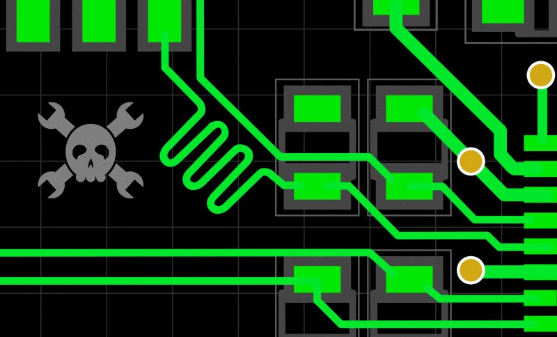
Last time, we looked over diffpairs, their basics, routing rules and the notorious tolerances of PCIe when it comes to diffpairs. Now, let’s take a look at the exact signals that make PCIe tick, as well as give you an overview of which sockets you can get PCIe on.
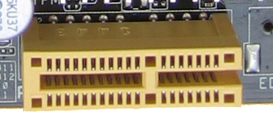
I separate PCIe sockets into two categories – desktop sockets, which are the usual 1x, 16x, or perhaps x4 PCIe sockets we see on desktop motherboards — and mobile sockets: mPCIe and M.2. There are also sockets like ExpressCard that are still found on some older laptops, but they have definitely fallen out of relevance. On mobile, M.2 is the way forward when it comes to PCIe – if you’re interested, I’ve written a short series talking about everything M.2 before.
On these sockets, most signals will be optional and some signals will be socket-specific, but there are some signals required in any PCIe device. Of course, the first group of required signals is the PCIe diffpairs themselves.
PCIe Is Just Spicy UART
Any PCIe interface has two kinds of diffpairs – TX and RX; for an x1 link, you will have one TX diffpair and one RX diffpair, and a x16 link needs sixteen of each. As you might expect, RX on one end connects to TX on another end, and vice-versa – it’s just like UART, but spicy. Of course, if you’re doing a PCIe extender or socket-to-socket adapter of some kind, you don’t need to do any swapping. If you’re designing a board for one of the PCIe-carrying extension standards, the usual naming is host-side. For example, say you’re putting a PCIe Ethernet controller IC onto a PCB that plugs into a desktop PCIe socket – connect TX and RX of the PCIe socket board to to your Ethernet chip’s RX and TX respectively.
If there’s strong indication that this convention has been violated, don’t fret – make sure to compare to an existing host or device, and see if you are able to determine whether the naming is as-expected or indeed, unexpectedly, flipped. Again, it’s just like UART! That said, there’s also AC coupling capacitors placed in series on both the TX and RX lines. Specifically in case of PCIe extension cards, be it M.2 or desktop PCIe, the convention is placing them on device-TX (host-RX) lines on the device board, and on the host-TX side (device-RX) on the host board. This alone is a pleasant divergence from UART when it comes to design and reverse-engineering.
The third kind of diffpair, one that’s invariably present, is REFCLK – a 100 MHz clock diffpair. It’s a speedy clock, and I’m not sure about its full purpose, but apparently, it plays a part in decoding the data on TX and RX, specifically, clock recovery – staying vital despite being orders of magnitudes slower than the GBit-range bandwidth of PCIe TX and RX pairs. Unlike with RX and TX, you cannot swap the REFCLK polarity willy-nilly. On the other hand, it won’t hurt as much if you have REFCLK pass through a set of vias or two in case you need to flip it – it’s just 100 MHz. Remember to respect your diffpairs, and you’ll be good.
REFCLK is required – except, theoretically, there’s cases where you can omit it, requiring both ends of the PCIe link to support recovering this clock from data passed through RX and TX pairs, or generate their own REFCLK. It sounds quite realistic, yet, REFCLK-less PCIe implementations aren’t really out there. Even SD-Express, a recent standard that brings PCIe to SD cards for blazing fast access speeds, didn’t go this route – the only consumer-available REFCLK-less implementation out in the wild is SATA-Express, a standard that became obsoleted by M.2 almost as soon as motherboards with SATA-Express ports hit the store shelves. As it stands, if you want your PCIe link to work, you absolutely need REFCLK.
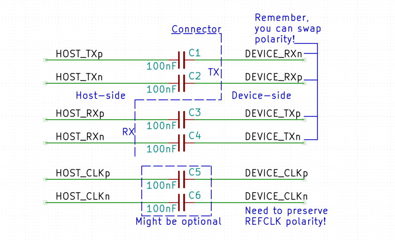
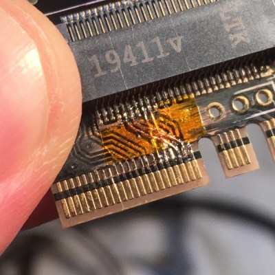
And now bit more about the capacitors. You need them on both TX and RX for the link to work, with ranges from 75 nF to 265 nF depending on PCIe link generation: 200 nF is a good all-around value and 100 nF will work in a pinch. Other than that, go for 0402 or 0201 package, and that’s basically it. REFCLK doesn’t typically need the capacitors, but they shouldn’t hurt either, and certain devices might require them. Also, here’s something puzzling – there’s been at least one documented case of a cheap mass-manufactured WD SSD seemingly omitting its TX-side capacitors, failing to initialize with a custom PCIe host board up until extra capacitors were added on the mainboard side. It’s not something you should do by default – merely a peculiarity that one manufacturer had the gall to create.
The Few Signals Necessary
Then, there’s a trio of single-ended control signals – CLKREQ, PEWAKE, and PERST. CLKREQ is used for power saving – the device usually sets CLKREQ low to start receiving REFCLK, and is able to de-assert CLKREQ (set it high) to signal the host that the host can stop providing REFCLK, saving power. The CLKREQ signal is peculiar – it’s present on mobile devices, but isn’t used on desktops, to the point where desktop PCIe slots didn’t even initially have a dedicated pin for it. As a result, the USB3-cable-perusing miner “GPU riser” boards do not pass CLKREQ through – only PEWAKE and PERST. If your host has a CLKREQ pin but the device doesn’t, ground it; if your device has a CLKREQ pin but the host doesn’t, ignore it, otherwise, connect them together.
Well, if the corner-cutting miners bother to pass PEWAKE and PERST signals through, then they must be important, right? Let’s see. PERST is the reset pin for the PCIe link, and the host holds it low until all the clocks (including REFCLK) and power rails are stable and other requirements are met for the host to start talking PCIe; it’s also used for some low-power mode management. PEWAKE is used for power management just like CLKREQ, and does seem to be required as well – this is also a device-side-controlled signal. These two signals are a bit mysterious to me when it comes to ways you can omit them, so I recommend having both of them connected unless they’re outright unavailable on one of the ends.
Desktop slots also have PRSNT signals – depending on the link width, you have to short PRSNT#1 to one of the PRSNT#2 signals. Not that this is required – PCIe is more than capable of detecting link width correctly; however, desktop motherboards do often need this in practice. It seems to be used for hotplug – something that PCIe is technically capable of, and which will even work if you use a system like Linux; Windows might just refuse to process PCIe hotplug unless you dance around your PC chanting magic words.
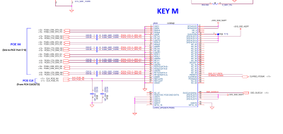
There’s I2C signals on both desktop PCIe slots and mobile slots like mPCIe or M.2. However, those signals are rarely ever connected on the mainboard – when they are, it seems to be either the mainboard manufacturer’s whim, or provisions for features like VPro. On server boards, they’re connected, causing fun things like some server-originated SAS controllers not operating on certain desktop boards with I2C wired up to the desktop-size slots. If you are wiring up a host-side PCIe slot, you don’t really need to wire I2C up, and if you’re wiring up a device, don’t expect I2C to reliably be there. Same goes for JTAG signals – they’re used in debugging or server environments, and are best left unconnected unless you’re certain your implementation benefits from them in the place where you’ll use it.
Mobile PCIe devices usually operate on 3.3 V power, whereas desktop devices can run from either 3.3 V or 12 V, for less or more powerful devices respectively. As a result, if you’re adding a desktop-sized PCIe socket and you don’t have 12 V handy, some desktop cards might randomly not work. x1 slots are expected to provide less power on 12 V than larger slots, and desktop motherboard manufacturers often take advantage of this leeway – if you’re designing an x1 card, don’t expect it to provide the full 75 W (66 W at 12 V), and if you’re designing a motherboard with an x1 slot, the good news is that you don’t need to provide the full 75 W.
All The Different Link Widths
Both the host side and the device side can have different link widths – the choices are x1, x2, x4, x8 and x16, where the number indicates the amount of pairs being used; due to the way that a PCIe links function at the low level, these have to be powers of two. As such, don’t expect a x3 link to work if you somehow connect three lanes from a host to a device – it will downgrade to x2. PCIe is flexible with regard to link widths – the host and the device settle on the highest common denominator. No matter if your host has a x4 link and your device is x16, or your host is x16 and your device is x4, they will settle on a x4 link width, using four pairs, not bothered that one of the ends has twelve more to spare. There are very rare exceptions to this – namely, some server-purpose cards; that said, even those are cases of “x8 card won’t function with a x4 connection” and a 1x link will still work as a fallback.
This adds quite a bit of flexibility – if either side doesn’t have enough lanes to match the other, you can always expect at least an x1 link to work nevertheless. For instance, you can put a x16 GPU into a desktop x1 slot by cutting a notch in the slot, and perhaps shorting the PRSNT pins on the slot – though, make sure that your card doesn’t want more slot-provided power than your 1x slot is willing to provide, which might very well be the case if you’re plugging an extra GPU into a cut-up 1x slot directly! When it comes to desktop PCIe slots and cards, you will see x1, x4, and x16 physical slot widths, and x8 slots and cards being mostly a server occurrence. There are some low-end GPUs that are actually x8 cards, but they use x16 physical slot card edge width, and same goes for x2 cards – they use x4 slot card edge width. You will rarely, if ever, see physical x2 and x8 cards or slots.
When doing a multi-lane link, you must make sure that you’re connecting lane 0 with 0, 1 with 1 and so on. There’s apparently an ability to reverse the entire link in case that can help you with your layout – say, in case of an x4 link, you could connect lane 0 to 3, 1 to 2, and so on. However, it’s not clear how widely that’s supported – it seems to be optional and not automagic.
And It Will Work No Matter What
Just like Ethernet, PCIe link speeds have been increasing with each generation, through gradual data rate increases, encoding type and other incremental improvements. Same story as with the link widths – there’s great forwards and backwards compatibility, a Gen1 device will work in a Gen5 slot, and a Gen5 device will work in a Gen1 slot, again, picking the highest common denominator. Of course, the link might end up being throttled from the expectation – if you plug a Gen3 x1 USB3 controller card into the Gen1 PCIe x1 slot on an old motherboard, expect the USB3 port throughput to be limited (and of course, same goes for connecting GPUs through a x1 link). However, this does mean that typically, you don’t need to worry about PCIe generations unless you’re aiming for a certain speed target.
Thankfully, if you have any PCIe questions that go seriously in-depth, there’s a lot of information online, and specifications for even the last-gen PCIe 5.0 are quite easy to find. It can be a bit dense compared to what you’re reading right now, but when you go in deep, it will help. Next time, let’s complete your mental map of PCIe, so that whenever you set out to stretch the limits of PCIe, you know how to approach it!


Thanks for this series, despite having used PCIe cards and servers in products we developed over many years, PCIe was still a bit of a secret world. One thing, in practice backwards compatibility is not always as reliable as you make out. For example some old TV receiver cards using the venerable saa716x chip stopped working in later generation HP servers because the chip apparently did not support newer link negotiation methods which if I recall correctly expected the chip to accept inverted polarity.
thanks. i’m surprised how much this series reminds me of reading the usb 1.1 spec. these designed-f
I hope this series of articles will take us all the way to the design of a basic, homebrew PCIe card !
PCI was rather out of reach for a hobbyist, with its complex signalling, but it seems PCIe is not so complex and that is good news.
I found it quiet easy to create PCI cards with a “Plx 9052” as interface between a aduC841 (8051) and the PCI-bus. This was in 2008..2016 for PCs on DOS and XP, where on DOS they where “full” PNP (Plug aNd Play) while in Windos it’s PNP was a pain, as in PNP = Plug No Play. Don’t remember it’s price tag (so it wasn’t expensive).
it won’t be “basic”, but it it will be something firmly within the reach of a hacker design… no more spoilers ^~^
How difficult it is depends what you want to get from the card:
1) Needs to be plugged in to m.2 slot, latency is not critical: use the USB 2.0 on it. Basically the same as using USB.
2) Needs to connect to ‘real’ pcie, performance is uncritical. Use some chip that converts pcie into something else, for example UART: http://www.wch-ic.com/products/CH382.html
3) Needs real pcie, performance is critical. Use a dedicated bridge chip or FPGA with serdes. Some advanced SoCs with pcie support can be configured as a device, although software support can be lacking (usually they are used as root complex for SSD/WiFi/…)
0402 metric or yankee units? Meaning go as small as possible due to characteristics X?
The *normal* 0402, whichever that one was =D Absolutely no need to go smaller than 0402/0201, mass-market PCIe devices don’t do that. As for the characteristic, don’t recall right now, but will recheck – one of the links in the capacitor paragraph might have more info!
Not answering your question, but to note I’m in a metric country, and I still use the imperial size for passive components. In my library I list them as e.g. “0402 (1005 Metric)”. Most online component suppliers do the same.
Which I find a bit opposite. In SMD land, all dimensions appear to be much more metric. Except passives, which are both dual named and worse, named with only one of to Mali g you guess.
I get the legacy bit, but at some point ya’ll just gotta let go ;)
” it’s just 100 MHz”. In digital signals, what matters is the edge rise and fall times, not the clock frequency. The faster the edge, the broader its frequency content. In RF-based communications, the information modulates the carrier, so the frequency of each component of the modulated signal is close to the one of the carrier. You may have a slow clock of, say, one pulse per minute; if its rise and fall time are very short, then you can 𝘴𝘵𝘪𝘭𝘭 mess up these pulses. The rule of thumb is that if the time it takes for the 𝘦𝘥𝘨𝘦—rising or falling—to traverse the trace is more than 10% of its rise or fall time, then the connection should be treated as distributed (transmission line); otherwise, it can be treated as lumped. So, here the question is how fast are the edges of this 100MHz clock of the PCIe bus.
If memory serves me right, the old PCI busses were unterminated, so at the end of the traces the ensuiong reflection doubled (almost) the pulse height and it was that reflected pulse that tripped the logic levels of the devices on the bus?
“You will rarely, if ever, see physical x2 and x8 cards or slots.” Nearly all USB Type E PCIe cards are x2 or x4 size. It was only in 2022 that the first x1 Type E card was produced, despite years of having x1 USB C cards available. Type E is just the internal / front port connector for USB C so there was no logical reason for *not making them in x1 size* for so long.
But at long last, anyone with a motherboard having only an x16 and x1 slots available and one or no Type E connectors can add Type E connectors for front USB C ports.
As for PCIe and hackers, will someone please design a USB C ExpressCard? I don’t care if it only goes as fast as original recipe USB 3.0 as long as it has a real USB C controller so it will work with things that don’t work properly (if at all) with USB 3 to C adapters.
Preserving polarity on REFCLK is not necessary. Swapping P/N here just results in a 180° phase shift. This doesn’t do any harm because there is no fixed phase relation between the clock and data signals. (Changing the length of the clock pair also shifts the phase.) Refclk is just the reference clock for internal high-speed clocks, but it isn’t used directly to sample/clock the data signals.
The more interesting aspect of REFCLK is that it’s not LVDS like the data pairs, but HCSL instead (with different termination usually).
that’s wonderful to know, thank you – will check ^^
> As you might expect, RX on one end connects to TX on another end, and vice-versa
Well, that explains why the M.2 slot on my CM4 carrier board doesn’t work… This is going to be tedious to bodge.
oh? got a schematic to cross-check? a m.2 slot should work TX-TX and RX-RX as the dia suggests! wanna pop into the HaD discord for debugging?
Thank you for the tutorial.