I’ve designed a few M.2 adapters for my own and my friends’ use, and having found those designs online, people have asked me for custom-made adapters. One of these requests is quite specific – an adapter that adds one more PCIe link to an E-key M.2 slot, the kind of slot you will see used in laptops for WiFi cards.
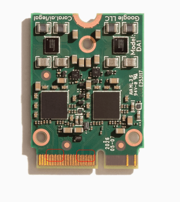
See, the M.2 specification allows two separate PCIe links connected to the E-key slot; however, no WiFi cards use this apart from some really old WiGig-capable ones, and manufacturers have long given up on connecting a second link. Nevertheless, there are some cards like the Google Coral M.2 E-key dual AI accelerator and the recently announced uSDR, that do indeed require the second link – otherwise, only half of their capacity is available.
It’s not clear why both Google and WaveletSDR designed for a dual-link E-key socket, since those are a rare occurrence; for the Google card, there are plenty of people complaining that the board they bought just doesn’t fully work. In theory, all you need to do to help such a situation, is getting a second PCIe link from somewhere, then wiring it up to the socket – and a perfect way to do it is to get a PCIe switch chip. You will lose out on some bandwidth because the uplink PCIe connection of the switch can only go so fast; for things like this AI accelerator, it’s not much of a problem since the main point is to get the second device accessible. For the aforementioned SDR, it might turn out useless, or you might win some but lose some – can’t know until you try!
Building Our Own Card
That’s a hacker-friendly problem we can solve for fun and learning opportunities! With a small enough PCIe switch chip, we could make an M.2 card PCB that also has an M.2 socket, putting a PCIe switch in between to split the incoming PCIe 1x link into two outgoing 1x links.
 What’s more, this problem has even been solved before. This exact adapter already has been made by someone online – however, it’s decidedly not open-source, and its creator has never started selling it, claiming lack of interest. The adapter we’re designing today, will be fully and properly open – anyone will be able to get their own adapter like this manufactured if they need one, learn from it, or remix it into something else.
On the PCIe switch side, I did mention a small, cheap and underexplored PCIe switch chip last time – the ASM1182e, which is able to create two PCIe x1 links out of one. It’s easily available on Aliexpress, used on many PCIe-splitting cards from China, it’s $6 after shipping, and it seems to be low-maintenance – small number of external components, standalone operation, simple wireup. Sadly, we just don’t have a datasheet for it that I could find – however, there’s quite a bit of information we can use to create our own boards, and I’ll show you how you might be able to design around chips even if you don’t have their datasheets.
Today, we’re solving a long-standing problem for a hardware niche, creating a M.2 adapter with three PCIe links in total, and reverse-engineering a PCIe switch chip with no datasheets available. I’d also like to make this board densely packed as a challenge, and show you what it takes, from a schematic page, to an assembled card.
Schematics More Open Than Expected
I’ll use one of my M.2 adapter designs as a base for this design – specifically, an A+E key to M-key adapter, letting you insert an SSD into a laptop’s WiFi card slot. That one’s a two-layer board because it could be, but today, two layers won’t do – this design will need four layers, as routing PCIe links properly and getting ground to everywhere would get way too intense otherwise! If you can reuse someone else’s design for your goals, absolutely do so – this one has tested symbols and footprints, meaning that there’s less variables for me to recheck! As a result, we don’t have to design an M.2 card from scratch.
The same goes for the reference schematic we can reverse-engineer the ASM1182 from – specifically, it’s from a mass-produced laptop. Today, we’re in luck – Clevo is one of the rare companies that has (or had) a tradition of publishing schematics for their laptops, likely helped by the fact that, unlike every other laptop manufacturer, they actually design their own mainboards. The only other laptop company I’ve seen publish schematics is Framework, whose mainboard is subcontracted (the norm in laptop space), and theirs is a partial one with all possibly-NDAed stuff removed. There’s no confidentiality markings of any kind on the schematic we’re looking for today – nevertheless, I’m not providing a link, but it’s undoubtedly the first result in your favourite search engine, especially if you look for P75xZM_ESM.pdf.
For the purposes of writing this article, it’s fortunate that this particular schematic does not appear to be problematic in any way. It’s apparently, quite uncommon for companies to issue takedown requests at schematic hosting sites, but these information-filled PDFs tend to be in a legal grey zone at best when it comes to distribution – you will see it argued that they fall under some form of intellectual property, and you might remember a “showing schematics on stream” dispute with Apple that thrust Louis Rossmann into the limelight. That said, if you personally ever use a schematic found online for reverse-engineering and design purposes, even if it has CONFIDENTIAL all over it, there’s no indication that you’re in any risk whatsoever – people have been doing that for ages with ThinkPads, Apple tech, and certainly random laptops here and there.
A Pinch Of Reverse-Engineering
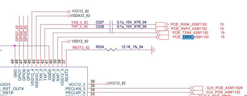
What do we get out of this schematic? Well, the entire page 93 of the datasheet is dedicated to the ASM1182, with a complete, tested and working circuit that actually was shipped inside a laptop. It’s not a datasheet, sure, but it has a symbol with pin names and it’s fully wired up, so it’s more than enough for us to copy the circuit; it even lists descriptions for strap pins, which is rare to find in schematics. Also, it’s basically the only information about it that I could find online, and I sure did search!
There’s one more source of reference – an open-source KiCad board with an ASM1184, a wonderful project by [will127534] that lets you connect four NVMe SSDs to a Raspberry Pi CM4, and our hacker has reverse-engineered the ASM1184 just enough to make a fully functioning board. There’s a bit of extra info on power requirements, too – for instance, we see that all the same-voltage power pins are joined together and it doesn’t seem like we actually need multiple 3.3 V or 1.2 V power rails, even if the pin names are different. Connecting all pins together is something that the laptop schematic also does, but in a roundabout way, so it’s good to have reassurance.
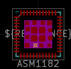 One thing the schematic doesn’t list is the ASM1182’s QFN package type – i.e. pad pitch. However, our ASM1184 shows that it has pitch of 0.5 mm, which I’d expect to stay the same within the IC family, and KiCad has 48-pin QFN footprints with 0.5 mm pitch that seem to fit the bill perfectly. Just like the Pi Pico, there’s 3.3 V and 1.2 V pins all around the package – for 1.2 V, I initially decided to designate an inner plane, but 3.3 V could go around behind the pins, between them and the ground pad. I’ve opted to decrease the ground pad’s size – you can do that reasonably safely on a QFN, and my aim is to be able to both put 1.2 V vias there but also be able to pull an extra track. 4 mm ground pad size works perfectly for this, going down from the original 5.3 mm.
In the end, even though we don’t have a datasheet and the chip is reasonably complicated, we seem to have everything we could need to design a board! You won’t always get this lucky – that said, now you know that inaccessible datasheets aren’t the end.
The Crucial Choices
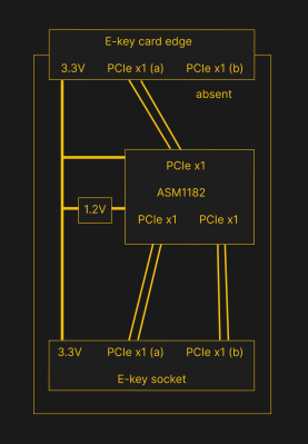
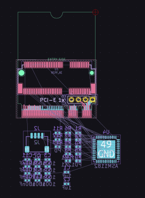
I got the ASM1182 symbol recreated in KiCad, and routing the schematic has been super simple – starting from the M.2 socket-to-socket adapter design I’ve had, I’ve added the ASM1182, wired up the signals of the three PCIe links, one to the card edge and two to the onboard socket, copied basically everything that the laptop schematic had, then started going through component footprint choices, estimating board component placement, and thinking through how the design could look.
 As usual, 80% of a successfully routed PCB is proper component placement, 80% is good routing choices, and the remaining 80% are mostly clairvoyance – if you aren’t good at the last one, don’t worry, just be prepared to redesign parts of the board once or twice.
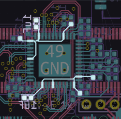
Here, component placement has been deceptively simple – I’ve taken an existing M.2 adapter as a base for outline, and assigned PCIe switch output links to M.2 socket’s link pins in a way that PCIe diffpair routing will mostly be short and sweet. After that, I’ve placed the PCIe switch on the bottom in a way that there’s plenty of space for PCIe diffpair routing on two more intense looking sides, and a bit of space on the other side for all of the PCIe switch configuration resistors. That said, it helps that I’ve been designing boards for a while and I have an eye for good component placement – if you’re starting out, you might not get it right the first time, so cut yourself some slack, ask people for a design review, and take note on what other people do when they design their own boards.
Such a board would more-or-less require a stencil for assembly – having a 0.5 mm pitch ASM1182 and an M.2 socket means that soldering iron assembly will be pretty effortful, and stenciling is fast in comparison. I’m going with 0402 components on this board – since I’m stenciling it anyway, there’s no good reason not to, and larger components would take way more space on the board. It’ll have to be dual-sided assembly, too – I’m not making a bet on having vertical space for any components under the inserted card, and having half of the space on the top layer occupied by the card edge and the socket puts us at a great disadvantage for single-sided placement. Usually, it isn’t as comfortable to stencil a board with components on both sides, but here I’d like to try and do it dual-sided anyway, and it should still be possible to stencil it despite any problems.
All in all, this is going to be a reasonably simple board to design and build, as long as we lay things out well! When routing such a board, you can start with the sensitive high-speed signals first while keeping the power rails and ground in mind, then route the power rails and ground while keeping low-importance signals in mind, and then, route the low-importance signals. Here, rotating the IC in one of the four directions solved most of the routing issues – putting both of the output PCIe links next to where they’re expected to be, and rotating the upstream link so that it can easily be routed from the card edge connector.
Capping The Power Consumption
Proper power is necessary for an IC, and doubly so for a fast PCIe switch. I have no datasheet to refer to when it comes to peak and idle consumption numbers, but in the laptop schematic diagram I have, it’s got its own 2 A linear regulator for the 1.2 V rail. I’ll personally go with a switching regulator, SY8089, a tried and true part from a well-known Chinese manufacturer. Since some of the pins are labelled as AVDD, I suspect some de-noising might be desired, but so far, both of the schematics we’ve seen, just join all power pins together with the non-analog-prefixed pins.
 As a rule, you’ll want one capacitor per IC power pin – my usual tactic is copypasting a ton of capacitors in the schematic, placing them around the chip according to the power pins I see, and deleting the extra ones afterwards. I’ve seen people use both 1 uF and 100 nF caps for decoupling, but it’s not clear there’s much of a benefit to 1 uF over 100 nF here – I’m going to use 100 nF caps in most places because they’re slightly cheaper, and add an 1 uF or two in places where current might have a harder time flowing, further away from the power source trace-wise. Of course, these are not exact values – it’s more of a range, and a capacitor’s presence at a power input is often way more important than its very specific value as far as IC decoupling is concerned, plus, the resulting capacitance varies wildly anyway, dependent on voltage applied, temperature, and the capacitor’s manufacturing tolerances. These are the kind of decoupling capacitor rules that I and many other people follow for own designs – if you’d like to learn more about rules of thumb and actual reasoning for decoupling capacitor choice and placement, there’s plenty of information out there to get you started.
Still, these are important capacitors, meant to keep a digital chip at a stable brownout-free voltage with its highly spikey current consumption pattern, supplementing the current that flows through the path from the power supply – a path which tends to be long-winded and electrically thorny, high inductance and all. In the end, I’ve made extra sure that all power pins have capacitors somewhere nearby, and added two 1uF capacitors at further-away 3.3 V and 1.2 V areas. This is, again, more of a vibes-based placement, but it tends to work well. Every decoupling capacitor has to have a great path to both its power rail and GND – vias will work wonders for GND as we have two GND layers throughout the board, and for 3.3 V with 1.2 V, traces under the IC or even on internal layers should work alright too.
Layout Done, Diffpairs To Go
Now, we have at least 80% of this board completed – it’s time to route it. Remember the routing order? High-speed first, then power and ground, then low-importance signals. If the high-speed signals don’t work, the board might as well be toast, and it’s pretty hard to bodge after the fact. If the power distribution doesn’t work, the board won’t work well, but it’s easier to bodge that. And, if low-importance signals are mixed up, you can generally bodge them easily!
As such, we start our routing with diffpairs – next week, we will plug board parameters into a calculator to get trace width and spacing, draw the pairs as properly as the board space allows us, and tune their length a bit – with a video demonstration, too!


Missed the perfect opportunity to mention the flexibility in PCIe links for polarity and count-up / count-down lane ordering. (Hosts and devices are expected to negotiate the polarity and the lane order, but lanes are required to remain in sequential order regardless of count-up or count-down). This makes it incredibly easy to route PCIe even when faced with swapped polarity or lane order on a chip vs socket.
PCIe lane reversal is optional, not required (at least… it was optional early, I can’t remember if it’s required now or not) – it’s not something you would want to put in a card that adds a PCIe port to an unknown device (or using a device with unknown specs, like here!).
You can generally get away with it because it’s pretty widely supported, but especially if you’re doing additional things like downshifting, you can run into trouble.
polarity swap support seems to be pretty universal! Now, lane reordering – that, I’m not sure about ;-(
Polarity swap is required by the spec and basically free to implement. Lane reordering’s optional and costs more since the lanes aren’t all independent (logical lane 0 is ‘special’ since it receives the start of data packet).
Polarity reversal is required by the spec and comes pretty much free in the receiver design. Reordering is not common in my experience, at least in embedded hardware.
Still waiting on someone to design an RP2040-based board in M.2 form factor…ideally supporting various key slots.
Throw on the same wireless module as the Pico W and a Qwiic connector, and they’ll sell like hotcakes.
That would indeed be very interesting.
Any ARM-based CPU with maybe ~1Gb of memory, wireless, u.fl connector and some flash or SD card socket. If anyone has seen or heard of something, please post below!
The RP2040 is a microcontroller akin to Arduino — it’s ARM-based, but not a full-fledged CPU.
But yes, what you’re describing would be interesting as well!
I’m imagining something like the VoCore, but in M.2 shape.
Maybe Cortex family CPU’s would be better, yes.
Possibly could put a CM4 on an M.2 daughter board, but it would be nicer to have it on one PCB.
The VoCore would be very easy to put onto a daughter carrier board in M.2 form factor, and would work out of the box using USB3.0 over the M.2 connector.
Honest question from an uninformed but curious reader: What can you do with something like that?
Like a SparkFun MicroMod? They have one with a RP2040.
Not sure about the hotcakes. Unlike QWIIC, I didn’t see much uptake of this “standard” so far, so I’m guessing they don’t sell that well either.
micromod is explicitly not compatible with laptop e-key slots, mind you – it uses M.2 for physical connectivity, but it isn’t compatible electrically at the very least.
Exactly what Arya said, re: MicroMod. I was super stoked when I first saw them, then disappointed. Even just having USB and maybe I2C exposed through standard M.2 pins would be huge.
As far as hotcakes go… I don’t know the exact statistics on hotcakes sales and perhaps was exaggerating… but maker-oriented SBCs are increasingly including M.2 slots of the A[+E] and/or B+M persuasion. I could see it being quite popular in that niche. Or for adding to developer laptops.
to allow 2 m.2 NVME drives to run in a PCIE x4 slot on a board without lane bifurcation (uplink is x4 and the card’s config implements 2 x4 downlink ports). I connected the m.2 B+M slot to a passive adapter which provides a standard PCIE x4 slot. Into that, I plugged in the PCIE x4 ASM2812 card and, into that I plugged in the boot NVME drive and a JMB585 SATA controller (m.2 B+M form factor). My informal tests show that, under load, SATA is never compromised, but the NVME drive does get slightly affected (it is not that fast a drive to begin with). That is when generating I/O on both devices.
Before anyone asks, I needed SATA port multiplier support and I know of no USB 3.x 10Gbps (or better) chip that can provide SATA ports that provide that functionality. I know of no older USB to SATA chips that do that either.
My comment got mangled. I need to rewrite the upper half (with some less context)
I bought a 100 $US ASM2812 PCIE 3.0 x4 switch card. This card to allow 2 m.2 NVME drives to run in a PCIE x4 slot on a board without lane bifurcation (uplink is x4 and the card’s config implements 2 x4 downlink ports). I connected the m.2 B+M PCIE x4 slot on my motherboard to a passive adapter which provides a standard PCIE x4 slot. Into that, I plugged in the PCIE x4 ASM2812 card and, into that I plugged in the boot NVME drive and a JMB585 SATA controller (m.2 B+M form factor). My informal tests show that, under load, SATA is never compromised, but the NVME drive does get slightly affected. That is when generating I/O on both devices.
Before anyone asks, I needed SATA port multiplier support and I know of no USB 3.x 10Gbps (or better) chip that can provide SATA ports that provide that functionality. I know of now older USB to SATA chips that do that either.
Thanks that was very informative! I would like to point out somebody has been making and selling these adapters for a while. https://github.com/magic-blue-smoke/Dual-Edge-TPU-Adapter.
Ye IIRC these folks are who I’d found during research phase for this article, that have built such an adapter! However, a) it’s not open-source, and b) the E-key version apparently won’t be sold to people. Effectively, a “screw you” to anyone who would want such an adapter – “I’ve developed it, I’ve tested it, but I won’t either sell it or share design files”. Such is not the case here, and, you get to learn from the design along the way, too! ^~^
I have designed a simple adapter into an E socket which has only one PCIe 2.1 lane populated. My adapter is being inserted into this socket and it contains a socket for NVMe SSD (M type). SSD has massive transfer capabilities, however the E socket is quite a bottleneck: 40MB/s is reached in best cases on both read and write. Even with PCIe 2.1, this should be peeked at maximum 500MB/s. We have done massive impedance requirements to the manufacturer, and it’s a 4 layer board. Impedances on lane traces are perfect, it was counterchecked. Any case, can this switch be interesting for me if I’m about to increase the transfer rate? NVMe has 4x lanes, from which now only 1 is connected. But I don’t really know SSDs heart. :)
I have connected SSDs with only one lane in embedded systems and this is likely not the bottleneck, as you said it should be around 500MB/s. Try another SSD?
I don’t know what hardware you are using, but on some CPUs there is a PCIe root core that has a low bandwidth connection to the memory bus. It is intended for things such as a WiFi card or IO card etc. If you connected one of these to the SSD it’s possible it will not work quickly.
Hi, thanks for confirming. The SSD itself is well capable of higher speeds, it’s a 1TB from Samsung (PM91A based), working crazy fast in other adapters. :)
Hardware is NanoPi R5C using Rockchip RK3568B2 (https://wiki.friendlyelec.com/wiki/images/3/35/Rockchip_RK3568B2_Datasheet_V1.0.pdf): it has
* 1x Multi-PHY2 providing PCIe2.1 with 1 lane (5.0Gbps per lane per direction)
* 1x PCIe3.0 PHY with 2 lanes (2 PCIe with x1 or 1 PCIe with x2)
According to R5C’s schematics (https://wiki.friendlyelec.com/wiki/images/4/45/NanoPi_R5C_2209_SCH.PDF), they wired the PCIe2.1 (1 lane 5Gbps /pg.8/) to the E socket (pg.18).
I asked the manufacturer (PCBWay), to impedance match my PCIe traces (clock, rx and tx pairs ) to 85Ohms +/-10% differential impedance. They theoretically have done it correctly, based on their report.
PCB is 4layers, so there should be no issues with proper reference planes underneath these traces.
`lspi` confirms the SSD’s PCI bridge “LnkSta”:
> LnkSta: Speed 5GT/s (ok), Width x1 (ok)
However the disk read: 170MBps (~1Gbps), and disk write: 50MBps (~400Mbps).
Test was done between this Samsung SSD and local storage (eMMC).
Just for your note uSDR is OK with just one lane PCIe 2.0. So you’ll be Ok with that in 99% cases. We routed the second lane because the FPGA we’re using has 2 lanes, so why just waste it? And this second lane is routed properly in our M.2 B+M to M.2 E adapter and PCIe x4 development board so you’ll get PCIe x2 2.0 connectivity. Since the uSDR board is designed for embedded use you can use the second lane for something else in your design :)