
After years of seeing people showing off and trading their badge Simple Add-Ons (SAOs) at Supercon, this year I finally decided to make one myself. Now for a first attempt, it would have been enough to come up with some cool PCB art and stick a few LEDs on it. But naturally I started with a concept that was far more ambitious than necessary, and before long, had convinced myself that the only way to do the thing justice was to have an onboard microcontroller.
My first thought was to go with the venerable ATtiny85, and since I already had a considerable stock of the classic eight-pin DIP MCUs on hand, that’s what I started prototyping with. After I had something working on the breadboard, the plan was to switch over to the SOIC-8 version of the chip which would be far more appropriate for something as small as an SAO.
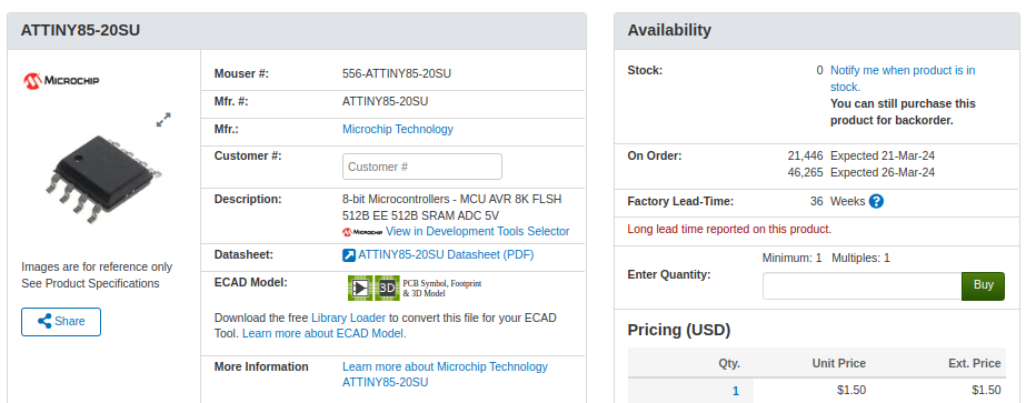
Unfortunately, that’s where things got tricky. I quickly found that none of the major players actually had the SMD version of the chip in stock. Both DigiKey and Mouser said they didn’t expect to get more in until early 2024, and while Arrow briefly showed around 3,000 on hand, they were all gone by the time I checked back. But that was only half the problem — even if they had them, $1.50 a piece seems a hell of a lot of money for an 8-bit MCU with 8K of flash in 2023.
The whole thing was made all the more frustrating by the pile of DIP8 ATtiny85s sitting on the bench, mocking me. Under normal circumstances, using them in an SAO wouldn’t really be a problem, but eight hand-soldered leads popping through the front artwork would screw up the look I had in mind.
While brooding over the situation my eyes happened to fall on one of the chips I had been fiddling with, it’s legs badly bent from repeated trips through the programmer. Suddenly it occurred to me that maybe there was a way to use the parts I already had…
In Case of Shortage, Bend Pins
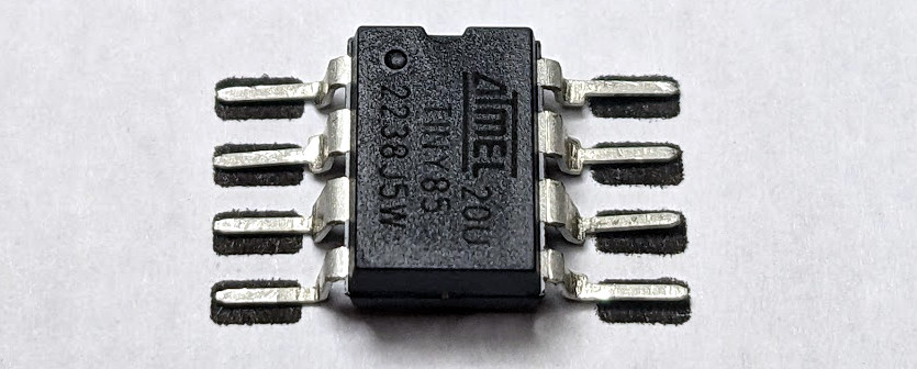
The idea was simple enough; I’d program the ATtiny85, carefully bend its legs outward, and then push the chip down firmly onto an ESD mat to get it as flat as possible. From there, I could snip the legs off with a side cutter, but I thought limiting the interaction between the chip and metal tools was probably for the best. As such, the result is a chip that’s flat to the PCB like an SMD component, but with leads that extend much farther out than any traditional package.
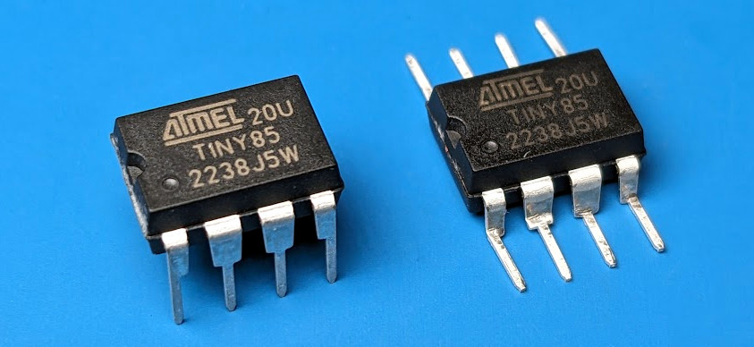
Obviously, the body of a DIP chip is still much larger than its SOIC counterpart. But it’s not like I’m trying to build a smartphone here, a small bump on the back of the SAO is unlikely to bother anyone so long as it doesn’t physically collide with the badge it’s getting plugged into.
But of course, a bent chip is only half of the equation. To put this into practice on more than a one-off basis, you’d need a suitable footprint so compatible PCBs could be spun up.
A Word on Footprints
If you only ever used jellybean components in your PCB designs, you could probably go for quite some time before having to design your own footprint. But eventually, it’s going to catch up with you. As the complexity of your projects increases, you’ll inevitably run into a part that doesn’t have a digital representation in your electronic design automation (EDA) tool of choice.
![]() With that in mind, creating custom footprints is a good thing to become familiar with ahead of time — nobody wants to have a project hung up as they struggle to get up to speed with a tool they never used before.
With that in mind, creating custom footprints is a good thing to become familiar with ahead of time — nobody wants to have a project hung up as they struggle to get up to speed with a tool they never used before.
We’ve previously looked at automated tools that will pull footprints from online repositories and convert them into something KiCad will understand. This is a great capability to have, but it’s not infallible, and there’s always a chance you’ll run across some oddball component out there that doesn’t have a publicly available footprint; so there’s still value in learning how to do it manually.
As this is a pretty simple footprint, it’s a great example to get started with. Even if you don’t plan on smushing your old DIP8 chips into service as makeshift SMD components, I’d invite you to follow along here if you’ve never used KiCad’s footprint editor. While not presented as a step-by-step guide, it should at least help you wrap your mind around the workflow.
Running the Numbers
Under normal circumstances, the first step in making a footprint would be to consult the datasheet for the part in question. There, you’ll almost certainly find a diagram that describes in precise detail the geometry of the component. Assuming the datasheet is accurate and you don’t flub any of the figures, you should be able to make a footprint without ever having actually seen the physical part itself.
In this case though, our footprint doesn’t correspond with any proper package. With no handy diagram to follow, we’ll need to take some manual measurements before all is said and done. But it did start as a normal package, so the ATtiny85’s datasheet still provides some valuable clues.
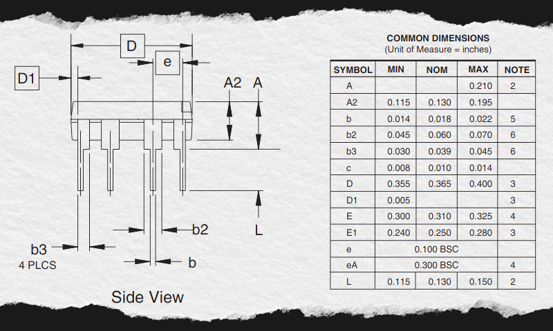
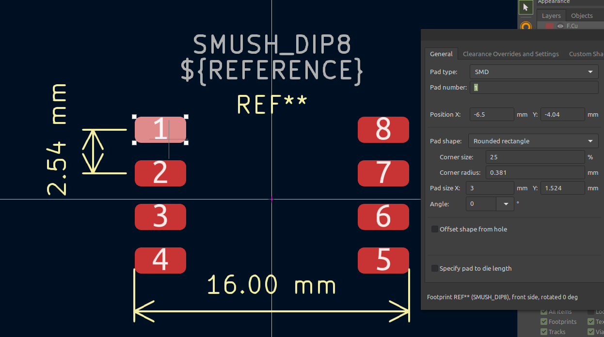
The main thing we’re looking for here is the size and spacing of the leads. This is labeled as “e” in the diagram, which corresponds to 0.100 inches, or 2.54 mm. BSC means “Basic Spacing Between Centers”, which indicates the measurement refers to the center point of each lead and not the outside edges.
As the leads have a stepped shape, there’s two figures given for each one: “b” for the thin tip, and “b2” for the wider base. We’re after “b” in this case, which the chart says could be anywhere between 0.014 and 0.022 inches. Helpfully, it also gives us a nominal value of 0.018 inches (0.45 mm). We can also see that “L” shows the nominal length of each lead, not counting the base, to be 0.130 inches (3.3 mm).
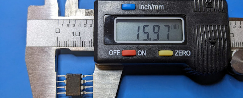
Given the length of the leads and the width of the plastic package, we could come up with a good estimate of the “wingspan” for our flattened chip, but it was just as easy to grab the calipers and check the real-world dimensions:
So where does that leave us? First of all, we ain’t going to space with this thing, so we can round off some of those numbers. This can buy a little of wiggle room, since the parts will be hand soldered, and just makes it a bit easier to wrap your head around. Second, let’s stop mixing units and just stick with metric since that’s what the board house is going to want anyway.
The end result: a footprint that has eight pads of approximately 3 x 1.5 mm, spaced 2.54 mm from each other, with a span of around 16 mm.
Putting Your Foot Down
The KiCad Foorprint Editor tool works more or less the same as the PCB Editor, and shares many of the same tools and icons. So if you’ve already got a couple custom PCBs under your belt, wrangling the interface shouldn’t provide much of a challenge.
Once you’ve created a custom library (which can be per-project, or global for all of your projects) and named your new footprint, you’re given a blank canvas on which to drop your pads using the appropriately named “Add a Pad” tool. After placing the first pad you can edit its parameters to give it the desired dimensions, and from then on, any new pads you place will have the same size and shape. The pad number will also automatically increment, though its up to you to make sure they match the part’s actual numbering scheme.
Using the various measuring tools at your disposal, getting the pad spacing where you want it is pretty simple. The most important thing to remember here is probably to set a reasonable grid size so you don’t have pads snapping to weird positions. For this example a grid size of 0.5 mm would be fine, but for finer pitched components you’d want to drop that down.
Once the footprint looked about right, I used the Print command to run off a 1:1 duplicate on a piece of paper and checked that the ATtiny85 physically lined up with what would be copper pads on a real PCB.
Lessons Learned
Now, I’m not claiming to be the first person to come up with this idea. Indeed, our illustrious Editor in Chief Elliot Williams says this wasn’t an uncommon practice back when hobbyists started dipping their toes irons into the world of SMD. So this is less breaking new ground, and more blowing the dust off a technique that’s been lost to time.
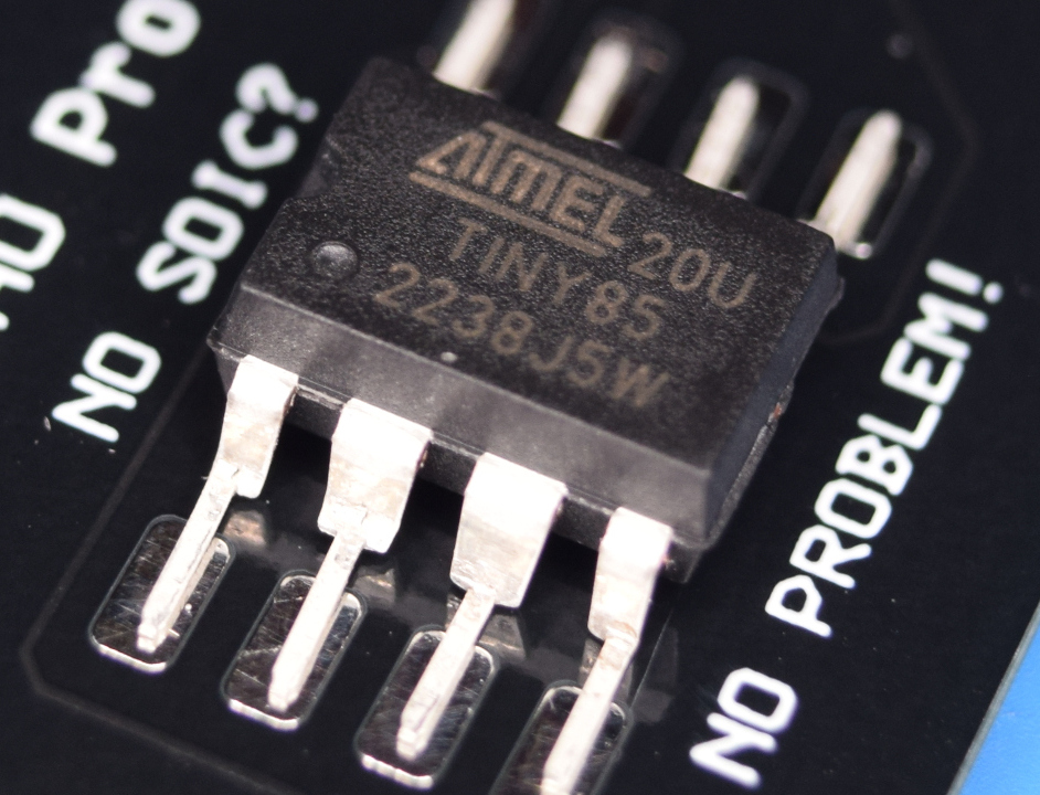 Was it worth the effort? As you can see from the image at the right, I did get PCBs made with this custom footprint, and I had no problem soldering these previously through-hole components as if they were supersized SMD chips. But ultimately, even the cost of the DIP8 version came out to be more than expected.
As of this writing, Digikey wants $1.66 each for the ATTINY85-20U. So while I did assemble several of the SAOs using this technique, in the end I switched over to the newer tinyAVR 2 family of chips. They don’t come in eight-pin flavors anymore, but the extra flash, UPDI programming, and lower cost more than make up for a little extra soldering.
So while it wasn’t quite the solution I was hoping for, it was certainly a successful hack and a good chance to brush up on some valuable skills. As any reader of Hackaday knows — the journey can sometimes end up being more interesting than the destination.


Clever hack. I think I would have cut the thin legs off and rolled the thicker portion under the chip so it looks more like a PLCC, but that would have meant using an oven or hot air for soldering…
I have done that for ever it feels like, and nah its a dip package you just heat the leg and the pad from the side, plenty of solder fillet
Doing that too. On prototyping boards it also has the advantage of much easier chip removals when you do not have to pull the legs through the holes (and then clean the holes to put legs through again).
Easy nice big packages, going well together with SMD passives. Makes board layouts much cleaner and easier to work on.
SOJ maybe?
I used to do this “back in the day”. It’s pretty easy to just roll the IC over a table and fold all the legs under too. Whether or not you need to clip off the thin parts of the legs depends on how hard you roll them.
You can get away with the standard DIP footprints too, especially if you use bigger solder pads. Hand soldering with an iron is beginner-friendly.
I know I did a couple workshops with this technique. These were hackspace-etched boards, single sided, and with tons of free pads to manhattan-solder stuff to.
Although if I were re-doing those today, I’d use 1206 SMT passives. Ironically, the hardest part of the prototyping method we used was holding the resistor leads in place without burning your fingers.
A number of years ago I experimented with etching my own PCBs for a Bob Blick style propeller clock using a PIC 16C84. I don’t remember the software I used for layout (it may have been paint) but I printed it out, did an iron on transfer, and traced the outline with the resist pen before exposing to a UV and etching….
All those steps later, I was left with a layout that was completely mirror flipped. I went to bed completely deflated, but woke up at 4:00AM with an idea: I could bend the pins on the micro around backwards, and everything would be fine.
Well, it worked.
I’ve had to bend the pins of a sot-23 transistor upside down and lay it down at a 45 degree angle to fix a prototype board with the wrong footprint.
Also handy when retrofitting a device from a coin cell to a Li-ion, and needing to cut voltage with a 3.3V LDO. Sometimes the LDO can be directly placed into the circuit. Other times it has to be “mirrored” this way.
https://cdn.hackaday.io/images/2320131583517075892.jpg
Picture of the PCB for a DEC H-500 Computer Trainer.
Yeah, it’s an ancient trick.
OMFG, that thing is amazing. I think those wire “overpasses” are the best thing I’ve seen all week.
Absolutely beautiful board!
Any reason not to go through hole with the DIP?
This is addressed in the first few paragraphs.
The link in the article that explains what SAOs are, shows an example board with a “SAO port which is a simple 2×3 0.1″ (2.54mm) header”. Given the SAO port is throughole header that doesn’t exactly have a low profile, it’s not obvious why the other components couldn’t be throughole, as well.
There are no through-hole components on the board, I’m using an SMD male header as well.
While there’s plenty of SAOs out there that manage to visually hide where the SAO header pins pop through, I couldn’t find a way to do it without compromising the look I was going for. The SMD header is naturally not as strong as the THT version though, and I had to make a jig to help align it during soldering, so it’s a trade-off.
Any reason not to flip your bent pin DIP upside down and go through hole with the chip body? Sure, the chip information would be on the back side but it’d make a thinner assembly.
DIL? Okay Boomer. :-D
can i use your soic breadboard tomorrow?
Say what? You Gen Z brat! 😁
Git off’n my comment lawn!
I think in fairness it is a demonstration of an approach if you have to make your own footprint for an odd component
Then there’s DIP-SM sockets.
Plenty of practice for CPUs.
Why reinvent the wheel? DIP cases modified for surface mount are quite common with optocouplers, KiCAD has the appropriate footprints out of the box (SMDIP-*).
Maybe he does not have DIP cases in hand?
Those are still intended for SMD packages though, so they are way smaller than this at 16 mm across.
Not to say it couldn’t work, but the point here seems to be that with the number being made (SAOs are meant to be distributed, generally) the solution needed to be something streamlined. Wrestling to get the chip on a too-small foot print might be OK once, but not 50 times.
I think I would have used the original footprint, sans holes, and just cut the legs off at the level of the PCB. Solder blob each leg and done.
Yep that works quite well that ro folding the legs under the chip
I was an early adopter of hobby SMD I hate drilling holes
it is a standard footprint, usually called gull wing
Amp and driver chips like it for some reason.
And optocouplers
My immediate thought was also to roll the leads under. That wouldn’t necessarily require hot air or reflow – I’ve soldered J-lead components by hand, and those leads are even smaller. Mind you, I wouldn’t wand to UNsolder such a component without hot air…
Ahhh… WordPress stikes again. I was replying, or trying to reply, to Pete, who posted the first comment.
As for WordPress, I’m NOT a fan of the new functioning of this page.
The ‘enter’ key no longer inserts line breaks for me, although I see it seems to be working for other commenters. And I miss the ‘keep me signed in’ checkbox. And has the font changed, or are my eyes just wonky today? I don’t remember it being this uncomfortable to read what I’m writing
Postings are mysteriously disappearing again. Maybe someone should run a consistency check on the database.
Keep me signed in works at not keeping me signed in. Every page asks me to agree to cookies. I have to shift-return for a new paragraph but even that might not work. Copy and paste from a text document even gets rid of the new paragraphs. So used to it unless I’m on my phone.
Then the return gives a new paragraph.
The font looks different, but it is more clear to me right now.
Slashcode is open source and has worked on bigger comment trees than Hackaday for over a quarter century now.
If Enter doesn’t work, it’s probably Shift-Enter, which I tend to use by default without even realizing it anymore.
Which fid already said, but I suppose it can’t be overstated? (Or I’m just a pointless obliviot.)
I have a desk calculator from the 2000s. Probably Canon. Single side PCB and the motor driver IC is a ULNxxx mounted just this way. The pins bent out and soldered as SMD. Funky.
Hey, that works! Good hack
Bend the legs totally flat, and have a square cutout in the middle of the footprint.
Lower half of chip body goes in hole, making extremely low profile.
So once the Hackaday Conference is over, will we get to see your SAO?
I was just going to ask if he’d bring it to Supercon. I’m another one who would love to see it.
We’ll get pictures for sure!
And anyone else who has an SAO that they’d like to show off — we’ll be populating the SAO wall again this year.
The plan is to have ~30 of them ready for Supercon to distribute. Clock is ticking though, so we’ll see how close I actually get…
There’s a Hackaday.io page for it, I’m just waiting for it to be completed before I made it public. All files will be supplied for anyone who wants to make their own, naturally.
I’m late to the game, but as others have mentioned, he made an 8 pin gull wing package. Used to be very common in the early days of SMT (I saw tons of these at HP in the early ’90s) because a lot of chip fabs just added tooling to the DIP8 manufacturing lines to form and cut the parts into a gull wing format instead of a DIP format. See: https://en.wikipedia.org/wiki/Lead_frame#/media/File:DIP16_Leadframe.jpg
Also, others mentioned SOJ, PLCC, and the “straight leads with body in a hole in the board” style. All common methods for prototyping. I personally use the SOJ style when forcing DIPs into SMT mode because I find it easy to just cut the leads little short and fold them under.
I like the details on making your own package in KiCAD as that is helpful for others. He may have been able to cheat bit using a gull wind pattern as a start, but all in all, he did well.
On the topic of chip shortages, a few years ago someone on the Parallax forums made a QFN44 to DIP40 adapter board when Parallax ran out of DIP40 chips. It actually resulted in a few other advantages and I believe he sold quite a number of them. Unfortunately, Parallax stopped the QFN package for the Prop1.
Another option is to lay out the board for an SOIC8 and use one of these: https://www.cimarrontechnology.com/product/browndog-201202-8-pin-dip-to-soic-8-adapter
Again, there are proper surface mount to DIP sockets available. Costs 50 cents apiece, but solves the problem more neatly.
Also costs the logistics of ordering and time for delivery. That can quickly get a few-cents component into a realm where it is easier to improvise with what’s on hand.
If you’re ordering parts anyhow, do you want to invest the time into folding pins by hand, or pressing chips into sockets? There’s a breakeven point where the extra setup time cost as much as the socket.
De-cap the thing, try to preserve the gold wirebonds :D
Maybe I missed it in the article but why not just use “DIP-8_W8.89mm_SMDSocket_LongPads”?
It’s in the standard Kicad libraries.
Nice and useful tutorial on creating footprints though
Thanks for the keyword! This will be very useful, for me at least :-)
Sort of in the opposite direction, but:
I imagine it would be possible to dead-bug a DFN, QFN, or VQFN chip with some careful micro-soldering and very fine wire. Though, you’d probably want to glue the package down and that would make it hell to remove.
Jep. Had to that once on a prototype. A 2×3 mm qfn chip with the pinout in the docs shown BOTTOM UP. thanks guys…