Hackaday Links Column Banner

Hackaday Links: June 8, 2025

When purchasing high-end gear, it’s not uncommon for manufacturers to include a little swag in the box. It makes the customer feel a bit better about the amount of money that just left their wallet, and it’s a great way for the manufacturer to build some brand loyalty and perhaps even get their logo out into the public. What’s not expected, though, is for the swag to be the only thing in the box. That’s what a Redditor reported after a recent purchase of an Nvidia GeForce RTX 5090, a GPU that lists for $1,999 but is so in-demand that it’s unobtainium at anything south of $2,600. When the factory-sealed box was opened, the Redditor found it stuffed with two cheap backpacks instead of the card. To add insult to injury, the bags didn’t even sport an Nvidia logo.

The purchase was made at a Micro Center in Santa Clara, California, and an investigation by the store revealed 31 other cards had been similarly tampered with, although no word on what they contained in lieu of the intended hardware. The fact that the boxes were apparently sealed at the factory with authentic anti-tamper tape seems to suggest the substitutions happened very high in the supply chain, possibly even at the end of the assembly line. It’s a little hard to imagine how a factory worker was able to smuggle 32 high-end graphics cards out of the building, so maybe the crime occurred lower down in the supply chain by someone with access to factory seals. Either way, the thief or thieves ended up with almost $100,000 worth of hardware, and with that kind of incentive, this kind of thing will likely happen again. Keep your wits about you when you make a purchase like this.

Continue reading “Hackaday Links: June 8, 2025”

An Arduino Nano Clone In A DIP-Sized Footprint

Nobody doubts the utility of the Arduino Nano and its many clones, and chances are good you’ve got at least one or two of the tiny dev boards within arm’s reach right now. But as small as it is, the board still takes up a fair amount of real estate, especially on solderless breadboards during the prototyping phase of a project. Wouldn’t it be nice to shrink down the Nano just a bit and regain a couple of rows for plugging in components and jumpers?

It looks like [Albert van Dalen] thought so, and he managed to get a Nano’s functionality — and then some — onto a DIP-26 footprint. The aptly named “Nano DIP,” which at 33 mm x 10 mm — about the same size as the ATmega328 on the Arduino Uno — will tickle the miniaturization fans out there. The board is built around an ATtiny3217 and has almost all of the Nano’s features, like a USB port, reset button, built-in LEDs, 5 V regulator, and preloaded bootloader. Its big extra feature is the 350-kilosamples-per-second 8-bit DAC, while sacrificing external crystal pins and a 3.3 V regulator.

To make the board cheap enough to manufacture, [Albert] elected a minimum component size of 0402, which made squeezing all the parts onto the board challenging. The MCU barely fits between the header pin pads, and the Micro USB jack had to be a vertical-mount type. It does the business, though, so if you’re looking to free up a little breadboard space, check it out.

Chip Shortage Engineering: Misusing DIP Packages

After years of seeing people showing off and trading their badge Simple Add-Ons (SAOs) at Supercon, this year I finally decided to make one myself. Now for a first attempt, it would have been enough to come up with some cool PCB art and stick a few LEDs on it. But naturally I started with a concept that was far more ambitious than necessary, and before long, had convinced myself that the only way to do the thing justice was to have an onboard microcontroller.

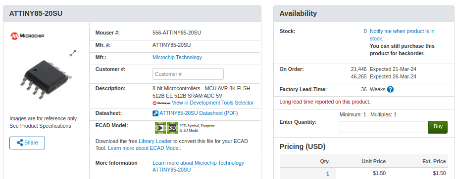
My first thought was to go with the venerable ATtiny85, and since I already had a considerable stock of the classic eight-pin DIP MCUs on hand, that’s what I started prototyping with. After I had something working on the breadboard, the plan was to switch over to the SOIC-8 version of the chip which would be far more appropriate for something as small as an SAO.

Unfortunately, that’s where things got tricky. I quickly found that none of the major players actually had the SMD version of the chip in stock. Both DigiKey and Mouser said they didn’t expect to get more in until early 2024, and while Arrow briefly showed around 3,000 on hand, they were all gone by the time I checked back. But that was only half the problem — even if they had them, $1.50 a piece seems a hell of a lot of money for an 8-bit MCU with 8K of flash in 2023.

The whole thing was made all the more frustrating by the pile of DIP8 ATtiny85s sitting on the bench, mocking me. Under normal circumstances, using them in an SAO wouldn’t really be a problem, but eight hand-soldered leads popping through the front artwork would screw up the look I had in mind.

While brooding over the situation my eyes happened to fall on one of the chips I had been fiddling with, it’s legs badly bent from repeated trips through the programmer. Suddenly it occurred to me that maybe there was a way to use the parts I already had…

Continue reading “Chip Shortage Engineering: Misusing DIP Packages”

Picture showing the way the cut-down piece of chip is soldered onto the mainboard - looking, indeed, like a QFN package.

Making A Handheld NES By Turning DIP Chips Into…QFN?

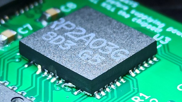
You can achieve a lot with a Dremel. For instance, apparently you can slim the original NES down into the hand-held form-factor. Both the CPU and the PPU (Picture Processing Unit) are 40-pin DIP chips, which makes NES minification a bit tricky. [Redherring32] wasn’t one to be stopped by this, however, and turned these DIP chips into QFN-style-mounted dies (Nitter) using little more than a Dremel cutting wheel. Why? To bring his TinyTendo handheld game console project to fruition, of course.

DIP chip contacts go out from the die using a web of metal pins called the leadframe. [Redherring32] cuts into that leadframe and leaves only the useful part of the chip on, with the leadframe pieces remaining as QFN-like contact pads. Then, the chip is mounted onto a tailored footprint on the TinyTendo PCB, connected to all the other components that are, thankfully, possible to acquire in SMD form nowadays.

This trick works consistently, and we’re no doubt going to see the TinyTendo being released as a standalone project soon. Just a year ago, we saw [Redherring32] cut into these chips, and wondered what the purpose could’ve been. Now, we know: it’s a logical continuation of his OpenTendo project, a mainboard reverse-engineering and redesign of the original NES, an effort no doubt appreciated by many a NES enthusiast out there. Usually, people don’t cut the actual chips down to a small size – instead, they cut into the mainboards in a practice called ‘trimming’, and this practice has brought us many miniature original-hardware-based game console builds over these years.

Continue reading “Making A Handheld NES By Turning DIP Chips Into…QFN?”

Open-DIP Surgery Cuts Retro Chips Down To Size

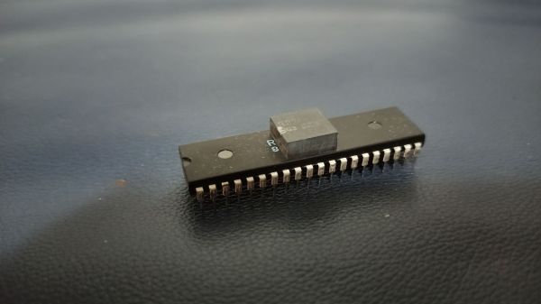
At least by today’s standards, some of the early chips were really, really big. They may have been revolutionary and they certainly did shrink the size of electronic devices, but integrating a 40-pin DIP into a modern design can be problematic. The solution: cut off all the extra plastic and just work with the die within.

Continue reading “Open-DIP Surgery Cuts Retro Chips Down To Size”

A 6502 Computer, With Acres Of Breadboard And Dozens Of Chips

Imagine you’re time-warped back to 1979 and tasked with constructing a personal computer. Could you do it? [RadicalBrad] thinks he can, and his 6502-based “Super VIC” build looks like it’s off to a great retrocomputing start.

Most emulations of old hardware these days go the FPGA route, and while we respect those projects immensely, there’s something to be said for applying a highly artificial constraint at the outset of a project. [RadicalBrad] chose to design like it’s 1979, and limited his ode to the machines of his youth to the 6502 CPU and logic and RAM chips available before 1980. The computer will support NTSC video output and 4-channels of 8-bit sound. No circuit boards will be used – everything is to be assembled on solderless breadboards. So far he has 48 (!) of them ganged together, which sounds like an enormous amount of space to work with, but he still found things crowded enough that some of the DIP bodies were trimmed a bit to fit more closely on the breadboards. The SRAM posed a problem, though, in that the 512K chips he wanted were not available in DIPs. To stay faithful to the constraints, he soldered the SOJ-packaged RAM chips into 40-PIN DIP headers – all 25 chips! We can’t recall a PC of the era sporting 12 megabytes of RAM, but no matter – it’s too cool not to love.

[RadicalBrad] has his work cut out for him, and this could take years to finish. We’re keen to follow his progress and can’t wait till it boots for the first time. Until it does, we’ll just gaze upon such discrete computing wonders as this almost-as-simple-as-possible computer, or even this delightfully noisy adder for a relay computer.

The Dual In-Line Package And How It Got That Way

For most of human history, our inventions and innovations have been at a scale that’s literally easy to grasp. From the largest cathedral to the finest pocket watch, everything that went into our constructions has been something we could see with our own eyes and manipulate with our hands. But in the middle of the 20th century, we started making really, really small stuff: semiconductors. For the first time, we were able to create mechanisms too small to be seen with the naked eye, and too fine to handle with our comparatively huge hands. We needed a way to scale these devices up somewhat to make them useful parts. In short, they needed to be packaged.

We know that the first commercially important integrated circuits were packaged in the now-familiar dual in-line package (DIP), the little black plastic millipedes that would crawl across circuit boards for the next 50 years. As useful and versatile as the DIP was, and for as successful as the package became, its design was anything but obvious. Let’s take a look at the dual in-line package and how it got that way.

Continue reading “The Dual In-Line Package And How It Got That Way”