We love that these days you can buy ready-made microcontroller boards that are very capable. But sometimes you need to — or just want to — do it yourself. Unfortunately, you really should design everything twice: once to figure out where all the problems are, and the second time to do it better. If you want to create your own board for the RP2040 then you are in luck. [Jeremy] has made the first (and second) iteration or an RP2040 board and shares with us what he would not do again.
In all fairness, he also has a blog post talking about what he did, so you might want to start there. However, we think his most valuable advice was his final word: Don’t fail to get started on your design. The longest journey, after all, begins with the first step.
His other advice is good, too. For example, don’t plug your new board into a computer because an error in the power supply could take the whole computer out. He also warns you not to do like he did and forget to order the $10 solder stencil with the PCBs.
Some of it is just good advice in general. For example — buy more small components than you think you need. There’s nothing worse than needing three resistors, having three resistors, and then watching one of the three fly across the room or stick to your soldering iron and melt into a pool of slag. Buy ten and you’ll save money in the long run.
In the end, the board did work and what he learned might help you if you decide to tackle a similar project yourself. [Jeremy’s] board is fairly large, but if you have an appetite for something smaller, check out the RPDot or the RP2040 Stamp.


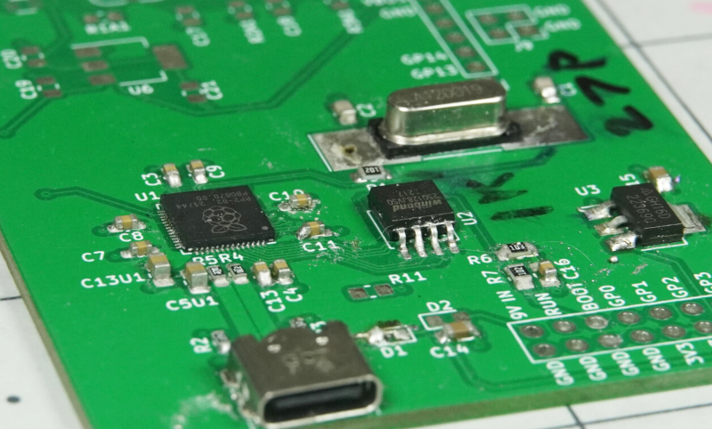
My number one recommendation regarding the RP2040 is to use a crystal oscillator. It may look cheaper to use a crystal and some passives, but for half the component count you get a stable clock that needs only a single trace brought out from the MCU and saves you debugging weird issues.
hmmm what kind of issues would that be? I’ve just been following the RP2040 hardware design guide (wonderful document, explains everything in detail and in plain language!) and 4-pin (3225 fp) crystals, and all of my RP2040 designs (think I’ve got like, 7) have worked wonders.
That’s EXACTLY the point – If it’s 4 pin, you’re an oscillator, not a simple crystal, which is a 2-pin component.
25 years ago I build a circuit with a simple crystal and the required inverters, capacitors and resistors. It was a nightmare to get working in any stable way.
Not necessarily. There are four-pin crystals with two NC pins. As always the datasheet is your friend.
For a modern chip, you typically only need two capacitors and the crystal itself. They include an oscillator circuit in the chip that does everything else.
ohh that makes sense, I’m confusing the two! yeah in that case, completely agree. Plus, these HC-49 crystals are just unnecessarily large.
There are tons and tons of crystals in a 4 pin package, some even have both pins on the same side so it matters what orientation you solder them.
This sounds like (maybe) ok advice – for a first-time hobbyist, but definitely not for someone that actually understands PCB design!
I didn’t even bother reading the entire thing, but I couldn’t agree more with Arya that the entire concept should be made in the first iteration! Not even just from a waste standpoint.
A perfect example I just dealt with was a review I just did for a customer – it was a simple microcontroller project with a bunch of outputs running different clocks. The board would initialize perfectly on startup, but outputs dropped to about 2/3 VCC.
One quick look and the culprit was a bunch of pi filters all over the board on input and digital and analog inputs to the MCU and other active ICs. A quick circuit analysis proved his values were incorrect for the speeds he was switching the outputs. All but the analog filter were really unnecessary, but he never would have known this if I hadn’t reviewed the layout with the rest of the components – and accompanying code!
An old boss of mine had this same mentality, just slap a basic sloppy design together and revise from there. He thought there was no way to get a good design in Rev 1. I refused to take this approach and you’d be surprised what you can accomplish in say 10 days vs a 7 day deadline. A few extra days gave me the time to do a full PDN analysis, EMC, SI, etc. and 99% of the time Rev 1 became the final product.
I could see where that approach might be useful for a brand new designer in a really complex setup, but keep in mind that EVERYTHING on the board is affecting EVERY other component in some way! A buck/boost converter will induce noise and requires careful placement and copper pours, each trace and component has parasitic RLC properties, noise is coupled from every nearby component/trace, and even the slightest shift can change a matched impedance. If you can’t route the board without chopping up the GND plane, you need a 4-layer design. There are about 1000x more things to actual PCB design than most people realize, even well seasoned hobbyists!
For parts, I wouldn’t even say to order 10 components if 3 are needed. Next time you go to order parts on Digikey, Mouser, etc., play around with numbers – MOST of the time I can buy 100 or even 500 resistors for the same cost (sometimes less!) rather than ordering 3! If 1-9 is $1.00 each, take a look at the price breaks at 25, 100, 500, etc.! It usually drops to about 50% if you buy 25, maybe 10% for 100, and under a cent for 500. This is a great way to build up your part library for future projects, and makes design easier on future projects of you already have the pinout and land pattern!
I would also suggest people watch some videos on different design aspects that may affect their boards. There are a lot of free videos and software utilities out there that cost nothing. Brush up on every aspect of your design, whether it be EMC/SI, antenna design, impedance matching and loading circuits, differential pairs, etc., etc. Trust me, it’s worth it in the end to spend an hour understanding how to match impedance on a differential pair like USB, even if you don’t think the speed warrants it – I see this all the time and the customer tells me it’s “only USB 2.0” but ends up being the reason they can’t read/write to the board without a programming utility.
I agree with your point in general, but the RP2040 has a specific complication: the analog circuitry on that chip is less mature other microcontrollers. This creates an unknown risk of system failure. Extremes of temperature, component tolerance, and chip process variations could cause the crystal oscillator to fail to start.
Evidence for the lack of maturity in the RP2040’s hardware includes:
•In addition to the standard load capacitors. the crystal circuit requires a series resistor to prevent damage to the crystal. No advice on how to calculate (or even tune) this value is provided [1].
•The RP2040 ADC’s accuracy was severely compromised by an analog circuitry design error, and this problem was not caught by RPi before release.
A crystal oscillator failure is a usually a device-killing failure, even if unlikely. Using an oscillator instead of a crystal avoids that risk (and takes up less PCB area as well).
[1] Hardware Design with RP2040, pg. 9 https://datasheets.raspberrypi.com/rp2040/hardware-design-with-rp2040.pdf
[2] Raspberry Pi Confirms It Is Investigating a Flaw in the Raspberry Pi Pico, RP2040 ADC. https://www.hackster.io/news/raspberry-pi-confirms-it-is-investigating-a-flaw-in-the-raspberry-pi-pico-rp2040-adc-95c393b55dfb
I absolutely agree. Doing all the checks before the PCB also lets you know where the tight spots are and so much more that you would otherwise probably need to discover for the next version anyway. Even if the “sloppy” prototype works, the production reject rate or warranty rate could be bad due to tolerances. I go even further, looking at the project holistically, including mechanical, power etc in the first (and only) pass.
The advice of “Do ask for help” is great and underappreciated – more people should seek out design review for their boards, it’s a wonderful way to make sure your PCB’s first version is actually functional!
On the other hand, the “Keep things simple” entry is plain wrong, you should not follow this part of the article, it will mislead you into wasting time and money on your boards with no benefit. In short, it suggests not adding the board’s desired features in the first board version, instead focusing on a ‘core’ part of the board and adding the actually important features in the next revisions when the ‘core’ part is done. This sounds like advice from the software world, and it does generally work for small-scale software, but hardware is very different, and this advice is badly counterproductive in the hardware world.
If you start with a simpler board and incrementally add features in the next revisions, you will waste a bunch of time and money on revisions that aren’t ultimately useful to you, as they don’t even contain the things you want to have that are missing from any generic RP2040 board. If you want to add audio jacks, add them in v1 and test them so that they’re ready for v2 – don’t wait to add them in v2 and then debug them in v3, because your v1 will be useless, your v2 will be disappointing, and your v3 will likely reach you by the point you’ve lost interest in the project you want to use these boards for. If you want to avoid major parts of the v1 core being wrong, again, ask other people to take a look at the finished design, or, better, copy the core part from one of the myriad of open-source KiCad boards on GitHub that have an RP2040 on them.
If you want to put a number of features onto your board, your first revision should contain them all – so that you can also start debugging all of your desired features one by one as soon as you receive the first revision board, have a bunch of fixes for the second revision, and likely settle at that. Or maybe, your first revision will only need a few bodges, or, none at all if you learn well enough from others’ PCBs! Then, you won’t even have to do a v2.
I think that the v2 board illustrates this problem well – it’s a custom RP2040 board alright, except notably less functional than anything you’d see on the market, as it only exposes 4 GPIOs and doesn’t do anything else. v2 could have had the battery switchover circuit *and* debugged audio output, and we would’ve had a way more interesting article. As an aside, don’t use 0805 components for RP2040 support circuitry, use 0603 at least – 0805 is barely easier to solder, and given how big it is, it will actually negatively impact your layout, as v2, again, demonstrates.
I agree, don’t go too simple. Get as much out of each board as possible before you junk it. Each iteration costs time and derails your thought process. Ideally, you do one proto and then a function board.
What I do is build the board much larger than needed. Give yourself lots of room to get in and measure (plenty of test points, too). Space for “dead bugs” and bodge wires. Some times I will put alternate approaches for a sub system and use solder jumpers or zero ohm resistors to isolate. I recently did this with 2 voltage regulators – one linear (known to work) and a switcher that I wanted to try. It’s ok to use 805 or even 1206 resistors and caps to make it easier to test and/or rework though once you gain some experience, 0603 are easy to work with. For a final RP2040 design, you probably want to use 0402s. A working design is easy to shrink.
+1 Hardware has much longer turnaround times than software.
You can add zero-ohm resistors so that you can easily disconnect different parts of the circuitry when needed. Zero-ohm resistors on your MCU GPIOs also allow you to easily swap GPIOs without having to scratch traces.
If you’re assembling PCBs yourself, you could start assembling your power supply and test it, then add MCU and test it and so on. It depends on the complexity of your board of course, but it can prevent you from having to throw away a board with valuable components because you forget some inner layer in the gerber data.
Some more tips:
1. Start with the raspi site. They have complete KiCad (And allegro) projects for you do download and modify.
2. RP2040 is a popular gadget. There will be a bunch of projects on github and such too. For example, the search below gives over 80 results. there must be some nice projects in there.
https://devbisme.github.io/RepoRecon/?topic=kicad&filter=desc:rp2040&sort=stars:desc
3. Put a decent GND plane in any uC project. Don’t cut it to pieces on both sides of the PCB.
4. Buy such a “resistor book” and “capacitor book”. Complete E12 and 100 or 200 pieces per value for about EUR25.
5. Do the initial power up always with a current limited power supply (something like 50mA or so). This often prevents IC’s from getting so hot they self destruct when there are solder faults etc.
6. Regarding crystals. Yes, these can be troublesome. They have a bunch of properties (series resistance, max power handling, and more) that can break your uC project if not done correctly. ST has for example has made cd00221665 which is a 59 page document about crystal oscillator design for their uC’s.
7. For very simple and one-offs it’s still cost / time effective to just use a breakout board and some matrix board to solder your circuit on. Unless of course your intention is to start with a simple project to get some practice with soldering QFN and such.
Great initiative of the OP to write up and sharing his experiences.
And great collection of additional advice & tips in the comments.
I’ll add some more random thoughts:
3.b: if you can at all, use at least a 4-Layer board stackup. Price diff to 2L is coming down rapidly.
8. Try to follow mfg design guides. But also sanity-check against other mfgs and more generic app-notes etc.
9. Don’t mess more than necessary with hand soldering (unless that’s a goal in itself). Prototype PCB-A (i.e. SMT assembly) services have come way down in price.
At least, consider buying SMT service for all the passives and other generic & boring dust & pebble components. It will get you to power-up smoke test & start of bring-up sooo much faster!
9.b : Also professional SMT let’s you use e.g. 0402, QFNs, BGAs etc challenging components, even if you’d find them difficult or “impossible” to hand solder. (Nothing is actually impossible, mostly “just” a matter of using proper tools, and gaining enough experience – through practice)
10. double/tripple/quadruple-check your footprints vs the compoents/variants you intend to use. Package, pinout, voltages & ratings.
10.b: if you have components already at hand, consider printing your board at scale 1:1, verify components fit on their footprints
10.c: set-up and run the ERC / DRC
10.d: verify your exported gerbers in a gerber-viewer
11. Someone else mentioned elsewhere – get somebody to review your board!
And finally – keep creating and building boards. More designs means more experience. Practice makes us better. And have fun!
>There’s nothing worse than needing three resistors, having three resistors, and then watching one of the three fly across the room
Everyone who builds scale models knows the terror of the carpet monster. A key part twangs off into the distance. You put panty hose over the vacuum nozzle, go over the whole room, and recover parts from your last three projects, but not the current one. Then: weeping.
Yes, what few people realize is that there is a dark matter interaction with your components as they leave the bench and head to the floor. Dark matter must be slightly heavier than air because as soon as the components approaches the floor not only does it travel much farther than possible with current physics models it also is able to hide around and behind things (something about dark gravity that I don’t totally understand) that normally do not interact with the known universe in any adverse way.
In any event, as soon as I drop something I focus all my attention on the path it is taking as it descends and even then my success rate in finding it is around 40%
Coincidentally I just found a Waveshare RP2040 board hiding under my small stack of drawers while looking for the schottky diode I just dropped.
Oh, it might be mine, dark matter, black holes, wormholes and all that stuff. Oh well, make good use of it.
But did you find one of my socks as well?
I found 16 left socks in the refrigerator (and some evidence of gravitational lensing in the butter), but I may be stuck in here now.
Darn, I’d always thought it was Duck Matter we were trying to avoid!
I’m going to move my workbench.
Thanks for the “pantyhose on the vacuum nozzle” tip!
As someone is currently designing a tiny (but still very useful!) RP2040 board a lot of these lessons ring true…
At this point though I have stopped bothering with solder paste. My components are so tiny that well tinned pads and some flux to hold everything down works great when reforming on a hot plate.
https://hackaday.io/project/192207-crapi2040
The not plugging into computer USB port advice is also questionable. The USB spec requires overcurrent and short circuit protection. So unless the board has another power source and may dump power into the port, for the most part, plugging an untested (but not maliciously designed) bus-powered device into a computer USB port is perfectly fine. I’ve done that many times including with first prototypes that have a short on 5V.
That TVS-diode (D5V0L2B3SO) he found to “work nicely” on the USB lines is actually a bit high capacitance (15pF).
Which is also indicated in that the datasheet doesn’t mention “USB” as an application area at all.
It probably “works” just fine, especially since RP2040 is only 12Mbps full-speed. But I doubt that he actually measured signal integrity a.k.a USB eye diagram.
As the data sheet hints, this part is considered “low” capacitance. There are also “very low”, “Ultra low” and “Extremely low” variants available.
There are rules of thumbs available, but generally go with “extremely low” (<0.5pF) for high-speed USB. Might get away with "ultra low" (0.5 – 1pF)
"Very low" (1 – 10pF) could be OK for fullspeed, at least the lower end, 1 – 3pF or so.
I think the generic recommendation should be : always check all datasheets for the components you're considering. Even boring/basic things like TVS diodes.
Make sure the datasheet lists your intended use (or something similar) in the "typical applications" section.
Thanks for the writeup!