Here’s a question for you: when your PCB has a ground plane layer, where do return signals flow? It seems like a trick question, but as [Kristof Mulier] explains, there’s more to return path routing (alternate link in case you run into a paywall) than just doing a copper pour and calling it a day.
Like so many other things in life, the answer to the above question is “it depends,” and as [Kristof] ably demonstrates in this concise article, the return path for a signal largely depends on its frequency. He begins by explaining current loop areas and how they factor into the tendency for a circuit to both emit and be susceptible to electromagnetic noise. The bigger the loop area, the worse things can get from a noise perspective. At low frequencies, return signals will tend to take the shortest possible path, which can result in large current loop areas if you’re not careful. At higher frequencies, though, signals will tend to follow the path of minimal energy instead, which generally ends up being similar to the signal trace, even if it has a huge ground plane to flow through.
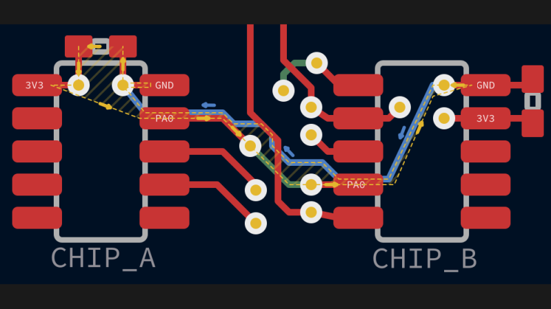
Since high-frequency signals naturally follow a path through the ground plane that minimizes the current loop, that means the problem takes care of itself, right? It would, except that we have a habit of putting all kinds of gaps in the way, from ground plane vias to isolation slots. [Kristof] argues that this can result in return paths that wiggle around these features, increasing the current loop area to the point where problems creep in. His solution? Route all your signal return paths. Even if you know that the return traces are going to get incorporated into a pour, the act of intentionally routing them will help minimize the current loop area. It’s brilliantly counterintuitive.
This is the first time we’ve seen the topic of high-frequency return paths tackled. This succinct demonstration shows exactly how return path obstructions can cause unexpected results.
Thanks to [Marius Heier] for the tip.


Not the best example there, though – if you care about that trace so much you shouldn’t be swapping layers if you can avoid it, period, especially on a 4-layer board where the impedance between top/gnd and bottom/gnd are very likely different.
Especially when you have an end-around route clear there. The via – pin – cap arrangement of the decoupling is also less than ideal.
People often care about more than one trace. So, example was on point. Exercise left to the reader to route the other traces they care about.
” Route all your signal return paths. ” Pure nonsense!!!
I mean, I route most high speed signal return paths…
because they’re almost always differential
To paraphrase Rick Hartley, a differential pair in a PCB with a ground plane underneath is not a single transmission line, it’s two single-ended transmission lines with a small amount of coupling between them. 85-90% of the coupling is to the ground plane, and the other 10-15% is to the other line in the differential pair.
https://youtu.be/QG0Apol-oj0?t=1549
That might have been a good rule of thumb 20 years ago. Not now. It depends on the stackup, geometry, and transmission line type. I tend to use only tightly coupled diffpairs.
Overall it’s just distance. If the complement trace is 4 miles away and the ground plane is 20, doesn’t take a YouTube video to see where the current’s going.
Replace that last link to the real one.
This kind of stuff can indeed be a headache at lower frequencies. Especially if you are crazy enough to dabble in sensitive Audio circuit design with FETs and/or Tubes. You will need to visualize return paths and plan the layout with that in mind.
My main approach is to carve up the main polygon for the pour. So instead of a uniform square form it is more jagged with gaps and slots here and there to nudge the return signals to take a similar route as the signals themselves. It ain’t as thorough as say manually routing (differential) signal return paths, but it is generally good enough making for an OK compromise.
Look up Robert Feranec on youtube, he has some really good videos about higher frequency return paths etc. He interviews people with decades of experience in the field.
This stuff is commonly misunderstood by even fairly advanced electronics engineers. Copper pours are usually no solution at all, and are sometimes even counterproductive. Return paths are often not properly thought out in four-layer boards either where the inner two layers are power and ground. Here are a couple of good videos about it (and there’s lots more where these came from):
Designing the Signal Return Path Through the PC Board – Susy Webb – Expert Live Training 11/18/19, on Altium’s channel https://www.youtube.com/watch?v=cAh4RyQHjOo
What Every PCB Designer Should Know – Return Current Path (with Eric Bogatin) 10/1/20, on Robert Feranec’s channel https://www.youtube.com/watch?v=icRzEZF3eZo
No GND vias wherefore switching layers? Hmmmm…
This seems like a convoluted way to just be mindful of via placement.
Hackaday Writers are poets with article Titles.
“For higher frequencies, it’s the path that minimizes the current loop area. The smaller that area, the less energy is lost to electromagnetic radiation.” Yeah, this is exactly the way of explanations when you want to spread maximum confusion. Well done!
Hi @Hans,
I’m the author. Nice to meet you.
The long explanation is this:
At elevated frequencies, the complex component of the impedance becomes more significant. In the case of a basic wire loop, its inductive resistance increases in direct proportion to the frequency. This resistance reflects the magnetic energy held within the loop, calculated by the formula 0.5 L I², where L denotes the loop’s self-inductance. L is connected to the squared magnetic flux density (B²), summed over all space. Therefore, given a choice, the return current prefers to travel as near to the signal trace as possible, reducing the loop’s area and, consequently, the space affected by a substantial magnetic flux density B. This results in a path of least inductance for the return. While the current disperses, it does so in a more concentrated manner.
I tried to shorten the explanation a bit. My apologies it wasn’t clear to you. How would you phrase it? Not arguing here – genuinly interested.
Hello Kristof,
this explanation is significantly improved. Truly! You should replace it with the one in your article. I would recommend omitting the energy part, though. Keep it as straightforward as possible. Most engineers think in terms of equivalent circuits, so an explanation using R, jwL, and 1/(jwC) would be adequate.
I really enjoyed Kristof’s article and it inspired me to take a deeper look at how the return currents behave in a simple benchmark setup. Looking at it in depth, it is surprisingly complex even for the most simple of setups.
https://medium.com/@andre.kuehne_67586/pcb-return-paths-visualized-622bb952e1ac