Last time, we went over switching regulator basics – why they’re wonderful, how do you find a switching regulator chip for your purpose, and how to easily pick an inductor for one. Your datasheet should also tell you about layout requirements. However, it might not, or you might want to deviate from them – let’s go more in-depth on what those requirements are about.
Appreciate The Feedback
There’s a few different switching regulator topologies. Depending on your regulator’s topology and how many components your chip contains, you might need some external components – maybe a Schottky diode, maybe a FET, or maybe even a FET pair. It’s often that the FET is built-in, and same goes for diodes, but with higher-current regulator (2 A to 3 A and above), it’s not uncommon to require an external one. For sizing up those, you’ll want to refer to the datasheet or existing boards.
Another thing is input and output capacitors – don’t skimp on those, because some regulators are seriously sensitive to the amount of capacitance they’re operating with. Furthermore, if you fail to consider things like capacitance dropping with voltage, you might make your regulator very unhappy – not that a linear regulator would be happy either, to be clear. We’ve covered an explainer on this recently – do check it out!
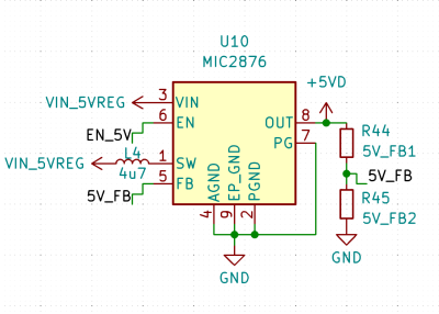
One thing you will likely need, is a feedback resistor divider – unless your switching regulator is pre-set for a certain voltage or is digitally controlled, you need to somehow point it to the right voltage, in an analog way. Quite a few switching regulators are set for a certain voltage output, but most of them aren’t, and they will want you to add a resistor divider to know what to output. There’s usually a formula for resistor divider calculation, so, pick a common resistor value, put it in as one of the resistors into the formula, get the other resistor value out of that formula, and see what’s the closest value you can actually buy. Don’t go below about 10 kΩ so that you don’t have unnecessary idle power consumption, but also don’t go too far above 100 kΩ to ensure good stability of the circuit.
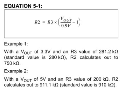
Some datasheets might even have a table of pre-calculated values for you to use. In that table, they might call for a very specific resistor value, but you usually can tweak that for the cases where all of your components have enough leeway. Would you care if your output was 5.1 V as opposed to 5.0 V, or 3.5 V instead of 3.3 V? Usually, you wouldn’t, and it might even be a little better if you increase the voltage a tad, so feel free to substitute that 157 kΩ resistor for a 160 kΩ one – just run the datasheet formula calculations to make sure you know what you will actually get.
Respect The Layout
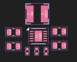
It’s not always that you have a layout example picture in the datasheet. For instance, it could be that you simply get a list of requirements for the layout, or even no requirements at all – sometimes you’ll just be reverse-engineering a board. Even if your datasheet is pretty good, sometimes, you will feel like deviating from the datasheet-provided example pictures. Here are some guidelines to know how to layout things safely.
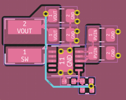
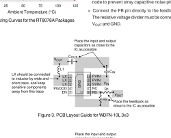
For a start, when it comes to placement of the feedback resistors, you’ll want to put them both as close as possible to the FB pin – the midpoint connection between them (the FB-connected track) is the sensitive part, since it’s high-impedance. So, the FB connection ought to be very short, and, of course, the GND connection has to be good – having a via to the GND polygon at the FB-GND resistor is a good idea. On the other hand, it’s okay to pull the VOUT connection for the feedback divider on the opposite layer through vias, because that is a low-impedance connection and it’s less sensitive to noise. If feasible, connect the VOUT connection “after” the capacitors, too, so that it isn’t measuring the point between the inductor and the capacitors, where current flows back and forth.
It pays to ensure that there’s uninterrupted ground on the layer directly under your regulator, as clean as possible, save for maybe that VOUT track, but even that can be worth routing out of the way. Switching happens at high frequencies, anywhere from 100 kHz to 2 MHz, your regulator datasheet will say which,, and it’s a noisy process. Anything less than a full and accessible ground polygon under the switching areas can, in the worst case, turn your regulator into a full-on noise problem in your circuit.
If your regulator has an ‘analog’ ground pad, respect that, and see what the datasheet says – the usual rule is to keep it away from the area where switching happens. Oh, and, it’s often that you need a ground fill directly under the regulator, on the same layer, too – for any switching that happens, whether it’s an internal FET and/or diode, or a driver for external FET gates. You can still try and protoboard a switching regulator circuit, but you’ll want to follow the next layout rule at the very least.
It’s important to put your inductor, diodes and all other components like capacitors as close to the switching regulator chip as you can. With current flowing through them at high frequencies, the connections between them can all become antennas, and the tighter you bundle all the components together, the smaller that antenna is – inducing less noise onto your circuit, which might interfere with WiFi or other wireless operation, analog measurements, or create weird faults in digital logic. Again, this is for you to mind in case there’s no layout recommendation – most often, there is one somewhere in the datasheet, so look out for it! As for traces, you want to provide a connection that’s as straightforward as possible. On connections where actual switching happens (the SW/LX connection from the chip to the inductor), use planes instead of tracks wherever you can.
In general, switching regulators are a bit of a noise source, so keep them away from analog parts; specifically, the SW/LX inductor-connected side. That’s not to say you can’t use switching regulators for anything where you do analog – a ton of modern microcontroller boards and circuits are using small switching regulators, including the Pi Pico. There will still be a bit of noise on the output compared to linear regulators, so if you want a low-noise rail in some part of your project, say, analog supply voltage for sensitive measurements, you can usually add a low-power linear regulator, or use a Pi filter, or combine both. Also, if you need to get plenty of low-noise 3.3V from a high voltage like 20V, you can also do conversion from 20V to 5V with a switching regulator, and then get 3.3V out of 5V with a linear regulator.
Having assembled your board, do you notice your regulator making audible noise? It’s usually not the inductor itself that’s to blame, since switching regulator frequencies are kept pretty high. More often, it appears that either the regulator’s duty cycle, or the capacitors are at fault, specifically, MLCCs, and the way they interact with your output load. It’s not an uncommon problem, though – here’s a page from Murata that tries to sell fancier “quiet” capacitors to you, a fun appnote from TI, and a PDF from Monolithic Power that suggests you treat your PCB as a musical instrument.
Make The World Go Round
 Switching regulators are very much a part of our arsenal and have been for a long time, as they’re fundamentally friendly for many cases where linear regulators fail us. Raspberry Pi has famously gone from a linear regulator to a switching regulator, because the 1A-only 1117 regulator they used, turned out to be a bottleneck, and we’ve seen quite a few Pi mods from before-2014 where people would replace the old linear regulator with a small switching regulator module for power savings and reduced heat. Another spot for switching regulators is battery-powered devices, where a linear regulator is often not a good pick because the wasted power decreases time on a single charge significantly.
It also pays to learn a bit how switching regulators work in principle, and, you can have some fun with the concept! Whether that’s making a switching regulator out of an opamp, using an ATTiny to do switching regulator duty, or repurposing the ubiquitous $1 switching regulator modules into negative rail power supplies, knowing the inner workings of a switching regulator makes your toolkit all that more rich. All in all, while a switching regulator might need a few more components, the extra effort is one hundred percent worth it, and if you have never added a switching regulator to your board before, your next design might be a good place to start!
Next time, let’s get down to business – pick a few switching regulators for common purposes, then pick components and do layout for a good few regulators at once, all done in an open-source design. After all, a picture speaks a thousand words, and I’ll make sure there are plenty of those.


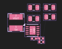
“It pays to ensure that there’s uninterrupted ground on the layer directly under your regulator”
The ground really wants to be right below the switch node, which goes from the regulator to the inductor. Obviously the node extends inside the regulator if it has internal drive transistors, so you need it under the regulator, too. The “layer directly under your regulator” is important – you don’t want to do top/VCC/GND/bottom if the regulator’s on the top (just put a ground pour on the VCC layer too).
Sometimes datasheets goofily recommend voiding planes underneath the inductor: this is because the plane effectively reduces the inductor’s value due to mutual inductance. However, this loss of inductance is almost always preferable to inducing eddy currents on all the other layers, which is what happens if there’s voiding.
There is one mistake in your layout, though! See where the Vout trace is going for the feedback? *Right over the switching node*! Yes, you might say “but there are planes between them” and that’s mostly true – its return current is going to be riding on the other side of the ground plane that the switch node’s on if there’s only one ground plane. It’s not needed – just route the trace away from the switch node. Route *everything* away from the switch node. Just imagine it like an angry giant yapping monster that everyone hates.
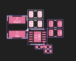
I think the biggest mistake in the layout is the position of the Vin capacitors.
The current with the largest variation is formed by the loop GND-(cap)-Vin-(HS-MOSFET)-SW-(LS-MOSFET)-GND. With a synchronous regulator (with internal MOSFET), the only off-die component is the Vin capacitor, and that should connect Vin and GND with the shortest possible traces. With your layout, the current either has to go around the capacitor pads, or through the vias – both increase the inductance unnecessarily.
I don’t understand your comment. How can the placement of the Vin capacitors could be improved ? They are already as close as possible to the Vin pins and they directly connect to the ground plane. The vias on the Gnd pin are useless in the picture, because we don’t see the bottom layer, but I *guess* they are just connected to a bottom layer ground plane directly
Flip them 180.
Trace their return current when the IC draws from them. The shortest path goes from the IC and around the cap (either through the plane or not, doesn’t matter).
Flipping them around shortens the loop because it shortens the distance from the IC to the negative of the cap.
If you look in most regulator layouts, the decoupling caps are like “back to back” input/output: they come to the same ground point. That’s why: cuts the loop size.
The original poster’s right, that’s a bigger deal, I just looked at the switch node. “Big” is relative here mind you – at these sizes it doesn’t have a huge effect, but it doesn’t cost anything.
Just remember if it’s too noisy… Just wrap it in some foil.
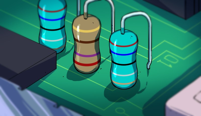
Is that a 390 MΩ resistor in the cover picture? Do they exist?
As a THT i have not seen them, but Stackpole has SMD 390M: HMC0805JT390M
I knew as i used a 360M from them lately and remembered them going even higher
Ohmite has a 10T resistor… or is that called an Insulator? ;)
UM050E100BKE
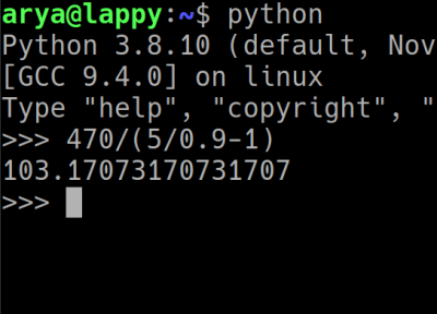
For an output of 5V, simplify to: R2 = R3 x 4.556.
Not sure why you flipped the multiply to a divide in your python code – were you starting with known R2 instead of R3?
Yes, I have a couple of high end gigaohm resistors in my parts drawers. 390MOhm is far from the end of what you can buy
OK, now I have to know… what the heck kind of circuit calls for gigaohm resistors?
Google gives me a lot of places to buy them, and how to measure them, but not much about why you’d ever need to use them.
Measuring very high voltages is one application, verification of your measurement for all kinds of impedance and dielectric spectroscopy methods is another that I have used them for.
Also used in IEPE charge amps.
People keep recommending to use buck regulators for battery powered devices, but most of them don’t actually achieve low quiescent current operation.
Suppose for example that you have a MCU that sleeps most of the time, but can’t be turned off, so power gating isn’t an option. A properly sized linear regulator can get you down to microamps in this case, while most switching regulators cannot, unless you turn it off, which isn’t an option here.
I would like to see a reference design that gets around this issue without adding too many parts, or some very particular chips that become unobtainium the moment you need them.
I used LTM8074 for this exact problem which achieves quiescent currents in the µA range. Not really a DIY case style, but works well if you can solder bga.
boost Dude, boost
I stay away from boost, because it has an inconvenient effect on lithium cell protection circuits.
When the voltage sags towards the end of your charge, the boost converter pulls more current, which makes the voltage sag even more and shuts down the battery before it’s empty. That’s why I’d rather have the cells in series and then drop down voltage, rather than cells in parallel and boost up.
The issue is mainly the dynamic range of current consumption. For many IoT devices, you have long period with tens of µA of consumptions (if not hundred) and communication period with 300mA peak consumption. A linear regulator that goes from 5V to 3.3V with 300mA has to burn >0.5W of heat. There are only few of them, and they do consume a non negligible quiescent current too in tens of µA too (like NCV8189 from OnSemi).
When running in 50/100µA range for the load, it’s only 280µW. A buck regulator with 95% efficiency will only burn 25mW when communicating (that’s 20x less than LDO), and consume 7µA while operating at no load (for example LTC3126, cf p6 of datasheet). That’s ideal for battery powered application. Even low cost converter that consume a huge 300µA will draw 1.5mW in sleep mode (that’s 5x higher than LDO). So for the LDO to worth it, you’ll need to spend 0.3% of the time communicating (and 99.7% sleeping). In that case, the LDO will consume ~1.8J over 1000s while the DC/DC will consume ~1.6J for the same time.
To put things in perspective, it’s ~10s of run time over one hour (since the µC will likely take few seconds to boot and rejoin the network, you only have maybe 6s of free time for communicate).
Most IoT protocols don’t allow such sporadic sleepy device:
– bluetooth maximum advertizing interval is 10s,
– Wifi 6 allows such intervals with TWT (not backward compatible) and weird to use in most case
– 802.15.4 could allow this for sensors, not for actuators (in that case, the maximum timeout before being ejected from the network is ~7mn IIRC)
– LoRa does allow whatever you want, so it could make sense here.
Some devices may transmit only when necessary, or only once every n-th cycle, so they’re sleeping most of the time, waking up for less than a second to measure something, and then go back to sleep. Then once in a blue moon they may spend a longer time to actually transmit data. 10 seconds of runtime per hour on average sounds about right for that case, and most of that time isn’t spent at the highest current draw either but something like 10-50 milliamps.
The once every n-th cycle is a typical case where you can’t use power gating because you’d erase the RAM contents, so you’d lose all the data you were collecting. You could add a FRAM chip, but then that’s adding complexity and cost in a different place.
>low cost converter that consume a huge 300µA
If your quiescent current demand is 300 µA then you’re wasting one typical 18650 lithium cell per year just to stay idle. But, that’s not the worst problem. The point of using a buck regulator is so that you could easily put more battery cells in series for a longer run time – something which a linear regulator can’t do. With a switching regulator, the load current out of the battery goes down and puts less stress on the batteries, which also makes them run longer in cold weather.
However, the switching regulator’s idle current doesn’t scale down with a higher input voltage. That means, if you put two 18650 cells in series in attempts to make the device run for longer, it just won’t. Both cells get the same 300 µA drain and they both go empty just to keep the regulator idling. You can add as many cells as you want, and they all go empty because of the high quiescent current – so a low Iq number here is paramount for getting any efficient use of your batteries.
> linear regulator that goes from 5V to 3.3V with 300mA
Linear regulators typically have lower parts counts and take up less space on the board, so it’s easier and cheaper to put them in parallel. For example, the NCV8189 you mentioned earlier shuts down to 0.1 µA. It’s is a 80 cent part in a 6-pin package, so you can easily have two and shut the other one down when not needed. You could also pick two dissimilar LDOs with one used for idling and the other for driving a large load.
> LTC3126
This is a ten dollar part with a 28-pin package, and requires yet more components around it to operate. It’s not really worth the cost.
“This is a ten dollar part with a 28-pin package, and requires yet more components around it to operate. It’s not really worth the cost.”
It’s a 42V input 2.5V A regulator with 2 microamp quiescent current and a bypass path. That’s *hard*. Of course it’s going to be expensive. If you want a super-cheap option, you shutdown the supply and ride it out. For lower total power, there are still plenty of other options at the microamp-scale that are dollar-ish: TI’s TPS6292xx series, Renesas’s RAA211xxx regulators, MPS MP2322, etc.
Getting down *below* single-microamp is very tough, obviously, but that’s to be expected.
>That’s *hard*
It didn’t need to be that overkill when the competition is rated for 5.5 V and 500 mA.
Yes. That’s my point. If you only need ~watt-ish power at a max ~5-ish V input, I don’t know why you’re complaining about buck regulator Iq.
You can *trivially* find fully-integrated buck regulators at the ~watt output level with Iq at the uA level during operation. and shutdown at the sub-uA level. I use the Torex ones all the time for that. They’re like, a dollar. They’ve even got the coils already on them.
Quiescent current on regulators basically scales with power capability.
Well, for my case, I need an input voltage that’s in the 12 Volt range, but not amps of current. More like 50-150 mA.
Point being that I want to add battery capacity by adding cells in series rather than in parallel, because it’s more complicated and finicky to divide the load between parallel cells while making sure they don’t discharge into each other or trip the cell protection circuits.
Yeah, I read. Which is why the list of all above are 15V+, uA scale quiescent, cheap, readily available, and simple. Just sort on Mouser. It’s a bit of a pain since Iq active is sometimes mixed with Iq shutdown. But that’s like, the most minor distributor gaffe compared to their typical eff ups.
As I said getting below single-digit uA takes effort, but that is almost universal. Chip manufacturers do press releases when their stuff hits nanoamps.
Some of the parts you listed certainly fit the bill – I should build a list for future reference. Thanks.
Selecting the correct regulator for the specific application is key. Texas Instruments has a vast selection of buck and boost converters that have sub microamp quiescent current and the same for shutdown current.
In a coin cell application the MCU can be powered directly from the battery and have sleep currents of around 2-3uA. That can easily mean at least a couple of years of sleep time. More power hungry devices can sit behind a buck/boost converter, that gets switched on only when needed.
Look at the regulator here. It’s not a buck regulator, it’s boost, but look at the quiescent current. It’s like 100 uA or so. So that’s bad, right?
Except the shutdown current is 3 uA from Vin and 5 uA from Vout, and it’s a bidirectional disconnect. So just… shutdown the regulator and have a few tens of uF on the output. If you can get your microcontroller to microamp sleep current, the regulator’s shut off and you can just wake it up again: 47 uF @ 10 uA will ride you through a second with a fraction of a volt drop. (I mean… this is almost exactly how light-load modes work on regulators).
Yeah, it’s not ideal, but this is a *5 amp* Random Boost Converter in a Hackaday article. Microamp-scale quiescent current regulators for low loads are common. It’s usually harder to get the uC and any supporting components to the level of the quiescent current of the regulator – you’ll bleed current through caps, diodes, resistors, etc. I’m usually chasing parasitic power draw from Random Crap for a while before I even think about the quiescent power of the regulator.
Generally the quiescent current of a regulator scales with the max output current, so yeah, you’ll have trouble if your weirdo circuit is like, drawing *amps* for only a few milliseconds or something, but at that point you’re going to have issues with circuits needing to settle due to the large current jumps anyway, and then you just do what I mentioned above: gate the power and ride through.
>It’s usually harder to get the uC and any supporting components to the level of the quiescent current of the regulator
Couple tens of µA for the entire thing is ok for most applications where you’re using regular rechargeable lithium cells. If you’re trying to shoot for more than a year of standby time, then the self-discharge rate of the battery becomes a greater factor and you have to start adding extra capacity anyways.
But as you said, it all adds up. You can have a capacitor that leaks 15 µA just because it happens to be like that. Another one won’t. You have to leave room for these kinds of “surprises” and variances within tolerances.
I mean, or you spend the money and design it in. That’s kind of the point: if you want it to work by design, you let the companies do the engineering rather than you. Lots of stuff has order of magnitude Iq/leakage current variations: you pay the money to get it reliably low.
I am the “company” that has to do the engineering, at least on the proof of concept level. Of course if I was given the budget, then I would contact big engineering companies and just buy the design, but then what would be the point of me?
No, I don’t mean the PCB design, I mean the chip design.
Switching regulators aren’t actually a “one size fits all” situation: if you *know* Vin/Vout and current requirements you can optimize the whole thing. But when you combine requirements, like, say, super light load current draw, low leakage, and low Vin/Vout ratio, you’re painting yourself into a corner without a lot of customers and so you’re not going to find many optimized parts, and they definitely won’t be cheap.
The reason these chips have a high Iq is because they’re *doing something* every cycle. In steady state in an ideal case (where you’re drawing the most you can) the duty cycle of the output switches is just given by the Vout/Vin ratio , and so if you’re not drawing any current, those switches need to *never turn on*. Otherwise they’re just throwing away power by switching.
Which is basically what the light-load stuff does for switching regulators: instead of varying the duty cycle to manage the current flow, you just… stop switching for a while. So essentially you vary the *frequency* of the pulses (or the period) – in some cases they call it “pulse skipping” or equivalent.
In your case you’re asking for an *exceptionally* long period, and that doesn’t make sense from a chip designer’s perspective. Now you need a huge freaking counter/timer/etc. to lower the possible frequency to absurdly low levels, when the user could just do it *for* you by actually shutting off the chip and get better performance because you could actually shut off the internal oscillator, comparators, etc.
> I mean the chip design.
I don’t quite understand what you mean by that.
What I was asking for is a reference circuit design – choice of regulator and the components around it – that would be a reasonable generic compromise for these kind of situations. Something that achieves reasonably low Iq with low parts count, without having to resort to tricks like toggling power and coasting through the brown-out, so we wouldn’t have to mind what exactly we’re powering with it. That way it could be a good default to start with, and then move away from if the task demands it.
“Something that achieves reasonably low Iq with low parts count, without having to resort to tricks like toggling power”
Again, to be clear, toggling power *is basically what the regulators are doing internally*! Look at the switching waveforms for “PFM” or “pulse skipping” or “Eco mode” or “burst mode” or “light-load mode” or whatever they call it – it’s *horrendous* compared to their normal PWM/forced conduction/whatever mode. “Running extremely intermittently” is literally the only way to get low Iq because it’s the switching that *causes* the Iq.
What I mean by it’s a chip design problem is that if you look at all of the performance corners of a switching regulator: Iq, efficiency, radiated noise, conducted noise, transient response – they’re all tradeoffs against each other. The chips that have higher Iq aren’t “bad”, they’re optimized for different points. You can’t get a magic unicorn regulator that’s just perfect at everything. Just not possible.
And the problem is that when you’re working in a regime where there aren’t other people doing what you’re doing… you’re just not going to get extreme optimized stuff that’s cheap. And that’s what this is. Switching regulators with super-awesome light load performance are all typically 5.5V-ish or so.
The regulators you’re looking for are basically all the ones with the light-load efficiency tricks. Anything that says any of the above tricks is likely going to have very low listed Iq, although generally it’s *only in the light load mode*.
>working in a regime where there aren’t other people doing what you’re doing
Which is odd, because nowadays lots of people are doing exactly this. Think, a GPS tracker for a bicycle that phones home after it detects movement from an IMU – it may spend months on idle and just checking the IMU every few minutes, which takes almost no power – but then suddenly it needs a watt to turn on the GPS and the cellular radio.
Though from what I observe, the other designers are solving the problem at the other end, like using high-capacity lithium thionyl batteries, or just accepting that you have to recharge every couple months.
“Which is odd, because nowadays lots of people are doing exactly this.”
No, they would just turn the regulator off and ride through with a 20 cent cap. If your design can’t take the voltage variation it wouldn’t be able to use the switching regulator anyway.
When recapping a SMPS, you have to choose replacement caps between several series offered by each manufacturer.
Some series offer higher temperatures (105°C and above), and differences in sizes (low profile, miniaturized) for when available space is a problem.
Some series also offer higher expected life ranges (1000, 2000, 5000, 10000h), which is probably great for devices expected to run 24/24 over years (but don’t know if the lifetime is also extended when stored unused?).
Beside that, other series offer low (or extremely low) impedance, or high ripple. It seems you have to choose one or the other, even if some manufacturers sometimes offer some high ripple variant of low esr serie (like Rubycon ZLJ which add high ripple to low impedance ZLH, but probably less than KXW High Ripple but not low impedance serie).
Most of the time, choosing lower (lowest?) ESR, high temperature (105°C) and maybe long life all seem to be smart choices, but i’ve read sometimes that for SOME caps, you don’t want too low ESR, otherwise you can have unwanted oscillations. If true, where are this ESR sensitive caps are located, and so which serie should be avoided or prefered there?
And i believe that in some places, High Ripple series could be recommanded too? But here is low impedance+high ripple is preferable than high ripple only series?
My wonderings could also extend to more general cases, like when recapping other boards (beside SMPS) in a device. I also wonder for example in which locations “For audio” caps could an improvement when recapping a cassette or reel to reel tape player for example. And if too low ESR could also be a problem in some circuits, or high ripple preferable in some others?
Some, older converters used voltage feedback instead of current feedback and require zero in frequency response of output filter, provided by ESR of output capacitors. This regulators are mostly gone but still sometimes seen in cheap or old designs.
Linear Technology (now Analog Devices) has some great app notes, and reference layouts. And their sales and apps engineers are extremely helpful. Love their parts (and switcherCAD/LTSpice)
OK now do an article on the only hard part. How to calculate/test the compensation circuit on many switcher ICs. Their datasheets gloss over this because it’s not straight forward.
But please keep in mind that Switching-PSUs need good filtering.
Not just to not break the law (TVI, RFI regulstions) but also in order to keep devices running smoothly.
Ripple and RF is the least you want to introduce to your device.
They can cause damage and malfunction.
In doubt, consider going for a conventional linear power supply with a good old 7805 or 7812.
It’s not the most efficient, but it’s clean by design. It doesn’t require complicated filtering like a switching power supply does.
It would be nice to see a follow up article on how to measure and validate a SMPS.
I recently tried designing a negative rail SMPS (Cuk, designed around an LT3757A). After struggling for a long time with the design and getting it built, it seems to work but I’d like to understand how to properly check things over the full range of operating conditions and understand the ripple (i.e. how would I know what to improve for rev 2?). The design is intended for a DIY audio project, but it’s something I hadn’t tried before and despite a lot of reading I am still second-guessing a lot of the design decisions. Any suggestions would be appreciated (I realize I saw this post a few days late though…)