
This article was prompted by a friend of mine asking for help on a board with an ESP32 heart. The board outputs 2.1 V instead of 3.3 V, and it doesn’t seem like incorrectly calculated feedback resistors are to blame – let’s take a look at the layout. Then, let’s also take a look at a recently sent in design review entry, based on an IC that looks perfect for all your portable Raspberry Pi needs!
What Could Have Gone Wrong?
Here’s the board in all its two-layer glory. This is the kind of board you can use to drive 5 V or 12 V Neopixel strips with a firmware like WLED – exactly the kind of gadget you’ll want to use for LED strip experiments! 3.3 V power is provided by a Texas Instruments TPS54308 IC, and it’s the one misfiring, so let’s take a look.
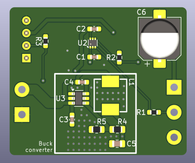
The design has an ESP32 on the opposite side of the switching regulator. For review purposes, let’s pull the regulator circuit out – disable all front layers (copper, silk, mask, courtyard and paste), hide vias, then box select the regulator circuit and move it out. I’ve also added net labels to the circuit – here’s a screenshot.
 There are things done right here, for sure, and a few things that could be the culprit in improper regulation. If you want hints, you can see TPS54308 datasheet, page 22, for layout recommendations. Both SW and FB nodes are pretty long, and the FB trace goes right next to VOUT – before regulation.
Furthermore, from the pinout and also the layout recommendations, it appears this regulator is designed in a way that all switching circuitry can be routed nicely. Yet, this design has the inductor go all the way to supposedly sensitive side. Thankfully, this is easy to fix.
Refresher – FB and SW traces have to be as short as possible, inductor as close to SW as possible, and the VOUT to FB connection can be a separate tracks on the other layer. With that in mind, let’s move the inductor to the other side of the regulator, move the FB resistors to the FB pin, and see how far we get.
My Take Versus TI’s Recommendation
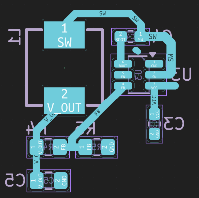
 This is my take. FB resistors moved to one side, switching components to the other, VOUT track on another layer. Add capacitors and vias as necessary, and pull tracks under components to get extra ground connections if needed. Of course, ideally, SW would be a copper polygon, and so would be VOUT. I’m also showing how EN could be pulled out, in case you needed that – in this particular schematic, EN can be safely left floating, but most regulators will want you to pull it either to VIN or to GND.
Since this is a TI chip, it also has a diagram for the layout recommendation! Let’s take a look how far off the mark we are, and it appears we aren’t that far. Curiously, it wants us to put SW onto another layer. Having switching current pass through extra inductance doesn’t sit right with me, personally, but my guess is that they want to minimize switching current flowing under the regulator, as the recommendation suggests.
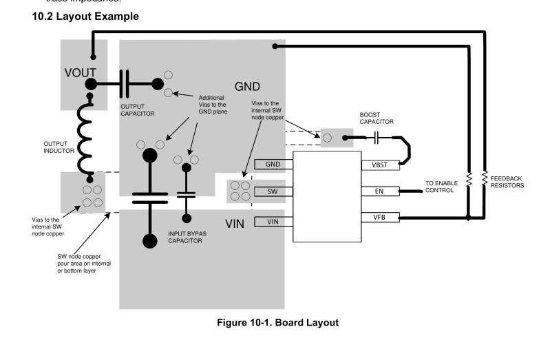
Another part that’s curious to me, is a suggestion for a Kelvin connection for the FB net’s GND pin. TI also publishes data for evaluation boards, and the TPS54308 has such a board indeed. Seeing on the page 13 of the evaluation board datasheet, I’m not quite seeing a Kelvin connection, unless Kelvin is the name of the engineer involved in designing the board. I do see that GND is tapped with a via far away from the area where switching happens, so it might just be that.
At this point, I’m curious whether my take is a dealbreaker, but since TI’s recommendations are available, I might just end up implementing exactly that and sending the files back. So, we take this circuit, implant it back into the board, order a new revision, and keep our fingers crossed.
A Pi-suited UPS, On A Stamp
A week ago, [Lukilukeskywalker] has shared a board with us, asking for a design review. The board is a stamp that houses a LTC4040 chip, and the chip itself is a treat. It takes 5 V, outputs 5 V, and when connected, it generates 5 V from a battery. It supports both regular LiIon, can do up to 2.5 A, and appears to be a perfect option if you want to power a Raspberry Pi or any other 5 V-powered SBC on the go.
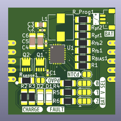
There are a few small nits to pick on this board. For instance, the connector for the battery is JST-SH, 3-pin, with one pin for BATT+. 2.5 A at 5 V means 12.5 W means up to 4 A at 3.5 V battery level, which might just melt a JST-SH connector or the gauge of wire you can attach to a JST-SH-sized metal contact. However, it’s switching regulator time, so let’s take a look at that specifically.
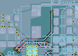 Here’s another thing you might notice immediately – lack of ground path from the IC’s ground connections, all the way under the switching path. In particular, the switching path is broken by a few traces, and it doesn’t appear that these traces must be there! Page 22 in the LTC4040 datasheet, which lists the layout recommendations, also stresses upon this, elaborating that “High frequency currents in the hot loop tend to flow along a mirror path on the ground plane which is directly beneath the incident path on the top plane of the board”.
Well, there are only two tracks that really interrupt the switching path above them, and both could be moved to the left. One of them is for a resistor that sets the charging current limit, and another goes to a castellated pad. Moving the latter is going to break the symmetry, but remember – it’s okay for a stamp to be asymmetric, that helps you ensure it’s mounted on your board correctly!
Sadly, while Linear Tech makes fancy tech, their evaluation board data isn’t as available as TI’s – there’s a PDF with schematics, but no layout data I could find. However, comparing to the pictures, you can see that the general layout of the switching area is correct, our hacker correctly uses polygons, the feedback circuit is pretty nice – it’s just these two tracks that are a bit uncouth when it comes to the switching regulator part of it. As for reviewing the rest of the board, you can read this article!
Towards A Powerful Future
Got switching regulator designs that didn’t quite work right when you put them to test, or that you’re yet to order and feel cautious about? Show them to us down below in the comments, and let’s take a look; your circuits deserve to operate at their best capacity possible.
And, as usual, if you would like a design review for your board, submit a tip to us with [design review] in the title, linking to your board files. KiCad design files strongly preferred, both repository-stored files (GitHub/GitLab/etc) and shady Google Drive/Dropbox/etc .zip links are accepted.


> it appears this regulator is designed in a way that all switching circuitry can be.
Can be what? I think the end of this sentence got misrouted :)
“this regulator” can be. It is correct
Can be designed
“can be routed nicely”, my bad, fixed!
Really enjoying this series! thanks for writing it up
+1 me too
Agreed! It’s turning out to be an excellent guide for people to improve their design skills, or at least get a better idea of the sort of questions you have to ask yourself when working on a design.
I’m learning quite a bit from the comments, too, thank you all so much for that =D
+1 me three
The TI example layout doesn’t make sense to me. What’s the reason for the long traces to the feedback pin? The entire area between the 2 reference points is a coil that can pick up unwanted signals and interfere with the feedback signal. I understand why the trace for VOUT goes all the way there, but the trace for the GND doesn’t make sense to me. Don’t you want your GND reference close to the output capacitor or close to the switcher chip?
Your layout makes more sense to me.
Same. I work for TI, doing switching regulator IC design stuff, and our layouts always look like Arya’s, with the switch node of the inductor up against the chip, to minimize loop area and radiated EMI. That node should be short and fat. Feedback and current-sense amplifier nodes through vias down into a lower layer that has some noise immunity through ground planes, sure, but we try hard to not be pushing the switch node through vias.
One thing that keeps coming up is: Does your “handle” “smellsofbikes”, refer to bicycles or motorcycles? As they have very different, uh, shall I say “fragrances”.
Oh no! A 3rd possibility just occurred to me! IIRC, back in grade school, there was a jock strap company named “Bike”!
Maybe the answer is more than I would like to know.
B^)
I’m not fond of that TI reference layout especially the switch node running on another layer.
Arya’s layout needs the polygon’s mentioned in the text to complete it and I think it’d be a better reference. Also I’d do a keep-out under the inductor to prevent the ground pour from flowing under it.
So, lets have a look at Arya’s layout, and see if it is actually better than the TI reference …
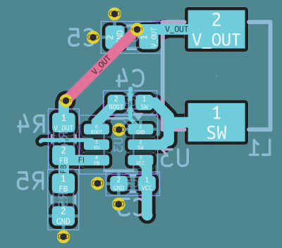
When the HS MOSFET is switched on, there is a GND return current from Cout (C5) to Cin (C3). The shortest path is the trace going under the BOOT capacitor (C4), but that trace is tiny – 1.5 mm long but only 0.2 mm wide (narrow). The other connection is via the GND plane on the bottom layer – but that has only 2 vias at each end (TIs SW trace has 4 each), the vias are oriented away, and the vias near C5 are behind the GND plane cut due to the V_OUT trace.
Some possible improvements for Arya’s layout:
1. Rotate Cout by 90′, so its GND is near the regulator GND. This also allows better placement of the vias. Additional benefit, the loop area is reduced.
2. Move the SW connection of the BOOT capacitor to the GND plane. This results in a small cut on the bottom layer GND plane, but earns you a much wider GND track on the top layer, where it matters most.
3. Rotate the feedback resistor to GND by 180′, and put it next to the other feedback resistor. This results in a much shorter connection to the Cout GND. Currently, it references the GND near Cin, at that has additional switching noise, due to the bad GND connection between Cin and Cout.
The area of the Vout-RFb1-Rfb2-GND-Cout-Vout loop going to FB is fairly neglegible, as long as you make sure:
1. both are routed next to each other
2. they are routed away from the switching current
The induced current will be tiny, and the additional voltage error, resulting from this current going through the feedback voltage divider resitors, is small compared with Vout.
Much more important is the loop formed by Vout-FB-Regulator-GND-Cout-Vout, i.e. mostly the white area enclosed between the GND plane and the two FB traces. This current is going into the high impedance VFb pin, and thus creates a much more significant error voltage.
I think that is what is going wrong in the original circuit. When you draw the loop of the switched on inductor current, and the loop of the feedback voltage, you will find the FB loop is enclosed by the inductor current loop. Everytime the High-Side switch is on, the induced FB voltage is added to Vout, and the switch will turn off much too early.
In the TI layout, the same happens in principle, but the induced current comes from the outside magnetic field of the switched loop, which is much weaker from the start, and decays fast when going further away.
I wonder what comes next as AI-assisted auto-routing able to dig into datasheets to extract recommendations, constraints, caveats, layout data and simulations…
For sure powerful tools like this will appear within two years.
A week or so ago I was looking for the LTC4040 test jig that I think used to come with then Linear Technology’s (now Analog Devices’) LTspice simulator. I remember having trouble with the LTC4040 example jig and gave up on it in favor of a homebrew SEPIC design. So last week I revisited LTspice. After a painfully long LTspice two-step update from ADI, I looked for the LTC4040 in LTspice and could not find it at all. And yes, I updated the components and libraries as well as the simulator software iself. The version after update was: Version (x64): 24.0.12.
I just started another update of LTspice. The first part of the update went way faster than before, but now I am stuck at the second Tools > Components update step staring at an empty dialog box that just says, “Updating example files…” for a loooong time.
Just now a small dialog box popped up in LTspice that said: “The update was compled successfully”. I clicked OK to dismiss the small dialog box, then restarted LTspice just to be safe.
After restarting LTspice, Help > About still said: Version (x64): 24.0.12. No wonder the first step of the LTspice update went so fast today! So I opened a new schematic in LTspice, clicked the Component (P) Icon and searched for the LTC4040. Nope, no LTC4040. All that turned up was a Coilcraft Inductor with the part number: LPS4040.
So it seems ADI doesn’t believe enough in the LTC4040 to include an example jig in LTspice any more. Considering that, it would be probably be a bad Idea to try using the physical part, especially at a price of $8.39 each.
“Both SW and FB nodes are pretty long, and the FB trace goes right next to VOUT – before regulation.”
Oh! This one’s easy! The FB trace is routed across the corner at one point,
and unless if you are “Madman Muntz” cutting corners often leads to failure!
B^)