It isn’t just a spy movie trope: secret messages often show up as microdots. [The Thought Emporium] explores the history of microdots and even made a few, which turned out to be — to quote the video you can see below — “both easier than you might think, and yet also harder in other ways.”
If you want to hide a secret message, you really have two problems. The first is actually encoding the message so only the recipient can read it. However, in many cases, you also want the existence of the message to be secret. After all, if an enemy spy sees you with a folder of encrypted documents, your cover is blown even if they don’t know what the documents say.
Today, steganography techniques let you hide messages in innocent-looking images or data files. However, for many years, microdots were the gold standard for hiding secret messages and clandestine photographs. The microdots are typically no bigger than a millimeter to make them easy to hide in plain sight.
The idea behind microdots is simple. They are essentially tiny pieces of film that require magnification to read. After all, you can take a picture of the beach and shrink it down to a relatively small negative, so why not a document?
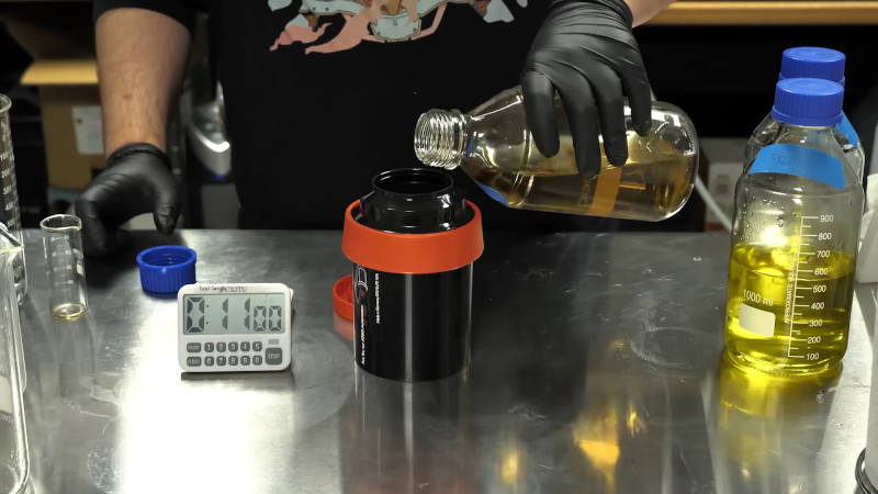
The example microdots use ISO 50 film to ensure a fine grain pattern, although microfilm made for the task might have been a better choice. Apparently, real spies used special film that uses aniline dyes to avoid problems with film grain.
However you do it, you need a way to take high-resolution images, put them on film, and then trim the film down, ready to hide. While microdots were put on pigeons as early as 1870, it was 1925 before technology allowed microdots to hold a page in only ten square microns in a 10×10 micron square. This was a two-step process, so between the film and the single-step processing, these homemade microdots won’t be that dense.
If all this is too much trouble, there’s always invisible ink. Or use a more modern technique.


” technology allowed microdots to hold a page in only ten square microns”
Please say more… this sounds improbable.
It’s impossible to focus light to less than a wavelength or so spot, or 0.4 microns, effectively the pixel size.
A microdot with an area of 10 square microns will be 3.1 microns on a side, and would contain a maximum of 8×8 discernable pixels. Can’t put very much information on that “page”.
Actually, that should have been 10×10 or 100 square microns. The Mikrat system from Goldberg supposedly could print the entire text of the bible 50 times in a square inch (although is that both books? Which version? I don’t know!).
More info… https://www.cia.gov/readingroom/docs/CIA-RDP80-00810A001000280008-2.pdf
Interesting document. Thanks for the link.
The device they describe puts 10,000 full-page images on a single 9×12″ plate. That would make each page image 3 mm high, 3000 microns.
My own experiments years ago got legible text at 25 microns per line, which would give (with line spacing) about 80 lines per 3 mm page, so about the same density.
Minor note, that spot size could be pushed a little smaller with oil immersion, although not enough to change your conclusion.
Both Tech Pan film and 25 ASA Kodachrome were capable of resolving 25 micron high text. Something like a lith film might be as good too, but I never tried those.
Kodachrome is long gone, but I still have 100 feet of Tech Pan in the fridge. I wonder if it’s still any good.
There was a “Mission Impossible” episode (TOS) where the “bad guys” used two microdots per message.
They needed to be overlaid and then would in a crossword puzzle like manner spell out the names of the spies.
Related to the latter, this is a nice read (was mentioned on HaD at some point IIRC): “visual cryptography“: https://doi.org/10.1007/BFb0053419
Nowadays you can get a 1TB micro SD memory card.
The chip used in that card is about half the size of the card, the other area is the controller chip. That’s 1TB in a square about the size of your pinky fingernail.
You can put that just about anywhere in your luggage and no one would find it. With 1TB you can store all of your information encrypted, including the linux OS, and boot from the drive itself.
I’ve always found that ‘kind of amazing.
(Although I’ve heard that PN junctions have a special resonance that can be detected by a a special scanner, a system sort of like a metal detector can be used to find hidden electronic devices. Don’t know how accurate that is, but a microdot could be detected by this method.)
There are special dogs that can sniff out electronic devices such as SD cards and USB flash drives.
https://www.techrepublic.com/article/electronics-sniffing-dogs-how-k9s-became-a-secret-weapon-for-solving-high-tech-crimes/
Except for the extremely low sensitivity (*), and if you could source it, holographic film would be great for making microdots. You could squeeze a 300-600 DPI 8.5×11 document into a one millimeter dot.
Of course in the digital age, we are tempted to say, well gee, why not just use a thumb drive? To which I must ask: Does any one know of commercial nonvolatile memory chips that fit in 1mm? For commodity for NAND Flash, bare die-size “sweet spot” is 100-180 mm^2. So at least 10x10mm (i.e. “big”).
(*) From: https://perg.phys.ksu.edu/vqm/laserweb/Ch-10/F10s5p2.htm — Holographic films is in the range: 2,000 – 10,000 lines per mm… Such high resolution film usually has very low sensitivity: Much less than 1 ASA, compared to hundreds of ASA (100-400) in standard photography film.
Answering my own question: Yes, On Semiconductor (and no-doubt others) makes a 512kbit i2c EEPROM in a 1.16×0.86mm WLCSP8, (wafer level, chip-scale package, with 8 solder balls). This will fit a fax-resolution image of a 8 1/2 x 11 page, assuming 2:1 compression.
If the best of that holographic film can resolve a line every 100 nm, but an oil-immersion microscope objective can’t do better than 200 nm, I don’t know how you’d actually observe the finished microdot, much less create it in the first place. Any ideas?
Deep UV.
Electron beam litho.
Synchrotron soft X rays.
Atomic force microscopy.
Electron microscopy.
And pretty much any way you’d make a modern integrated circuit.
Makes sense; I guess worst case that just adds a step on the making side. But for viewing, I guess you project deep UV into a phosphor sheet?
Microdots I came across looked way different and you ate em….
Those ones made everything look way different. :-)
Adox CMS 20 is a nice fine grain film for these sorts of experiments.
OK, here’s my question… If these are such good tech, why aren’t we storing data this way? God, can you imagine a QR code out of microdots? Be like some kind of infinite loop.