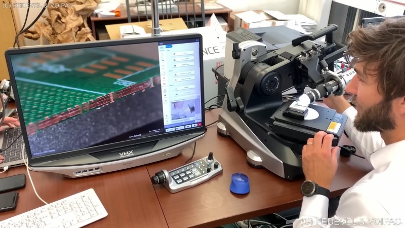
A word of warning before watching this very cool video on soldering: it may make you greatly desire what appears to be a very, very expensive microscope. You’ve been warned.
Granted, most people don’t really need to get this up close and personal with their soldering, but as [Robert Feranec] points out, a close look at what’s going on when the solder melts and the flux flows can be a real eye-opener. The video starts with what might be the most esoteric soldering situation — a ball-grid array (BGA) chip. It also happens to be one of the hardest techniques to assess visually, both during reflow and afterward to check the quality of your work. While the microscope [Robert] uses, a Keyence VHX-7000 series digital scope, allows the objective to swivel around and over the subject in multiple axes and keep track of where it is while doing it, it falls short of being the X-ray vision you’d need to see much beyond the outermost rows of balls. But, being able to look in at an angle is a huge benefit, one that allows us a glimpse of the reflow process.
More after the break
[Robert] also takes a look at other SMD packages, such as a TSSOP chip and a QFN package, as well as some through-hole terminals. He also forces a few errors, like misaligning leads or using way too much solder, just to show how fault-tolerant SMD soldering can be. The real eye-opener here was the excess tinning on the central pad of the QFN, which clearly caused problems by preventing capillary action from pulling the outer contacts down onto the pads. We’ve had that same problem ourselves, and seeing this makes us want to give that repair another go.
Kudos to [Roboert] for sharing these delicious views of what’s really going on when the solder starts to flow.


Really neat how it stays in focus no matter how you turn the stage or swivel the camera. Very smooth video!
The scope itself, used, is $3K on fleabay. The motorized base, used, goes for $8K.
I think you missed zero there. The VHX-7000 is well over $25k. There is a VHX-6000 on eBay right now for $24k.
Oh my god, that microscope. WANT.
In case you desperately need some up-close images, one option is to dismantle a cheap webcam. The lens assembly is usually held with a dab of glue, but it can be twisted off with enough force. Then you can adjust the focus distance to something like 1cm.
The image quality is nowhere near a decent microscope, but it can still be useful.
Telemicroscope close-telescope or something like that. Closeup with out being close up to the focal point. That’s some optics! Then the paired motions, excellent. Soldering stuff best views ever.
With all those degrees of freedom, I wonder how you avoid crunching the lens into the object being studied.
Notice it has equipment to do 3d scans with very precise scale measurements, implying that it has to know the distance of the lens to the object to get the scale right. I’d bet it’s smart enough to know where its lens is and when it’s getting too close to a sample
Even a 10X optical one is a great help.
I’ve had amazing success with using one of those cheapo HD usb microscopes held with an articulated fine adjustment probe holder. The listing boasted 40x-1000x magnification and while I can’t verify, I can say my only problem with hand soldering 0201 components is now solely down to my shakey hands. I’ve melted a couple spots on the cameras plastic housing but it was less than $30 so worst case I buy another one if it gets too bad. Making it autofocusing though is a cool idea and maybe I can slot it down on my long list of to-do projects.
The biggest trouble was trying to minimize the lag from the camera to attempt for a real time display. it works no problem on my android but I’m using a raspi I had lying around hooked up to an older pc monitor on a cheap counter weighted monitor arm. Playing with ffmpeg settings, I’ve been able to get lag under 1sec so for the entire setup coming to around $100 along with some already owned equipment its very serviceable. I expect if I was using something with more processing power, the lag would be even less noticeable as I expect it’s mainly from downscaling the 2k video to my screens 1080p.
I got to play with one of these at a convention a little while ago. They are VERY nice. Jealous
Fermi Lab developed a microscope to peer into the edges of Bump Ball Soldering (BBS) for Silicon Detectors bonded to PC boards 15 years ago. Looking into lines of pilers of trees. I developed a byfacial IR camera with separate IR frequencies that can look thru Silicon. This was used to check BBS mismatched to aluminum pads and under filling of thin layered Silicon Detectors also 15 years ago along with the system to peer at BBS edges. Pushing optical capablities has its limits.
Greg, 42 years at Fermi..
Our group built the Silicon Detectors that aided the discovery the Higgs Boson…
OMG… Surely I can think up enough applications besides PCB inspection to justify the investment in one of these. For example, I’d dearly love to get my micromount mineral specimens into the thing. Inquiry placed.