If you want to reverse engineer the boards in a modern console, you’d better have a lab, a lot of fancy gear, and a good few months to dedicate to the task. The humble PlayStation, on the other hand, is more accessible in this regard. [Lawrence Brode] pulled one apart and started documenting it as part of a grander quest for console understanding.
[Lawrence’s] ultimate goal is to create a portable PlayStation using original hardware. That is, rather than cannibalizing an existing console, he wants to build an original portable from scratch. He needed to understand the PlayStation to recreate it, so he started by analyzing the original hardware.
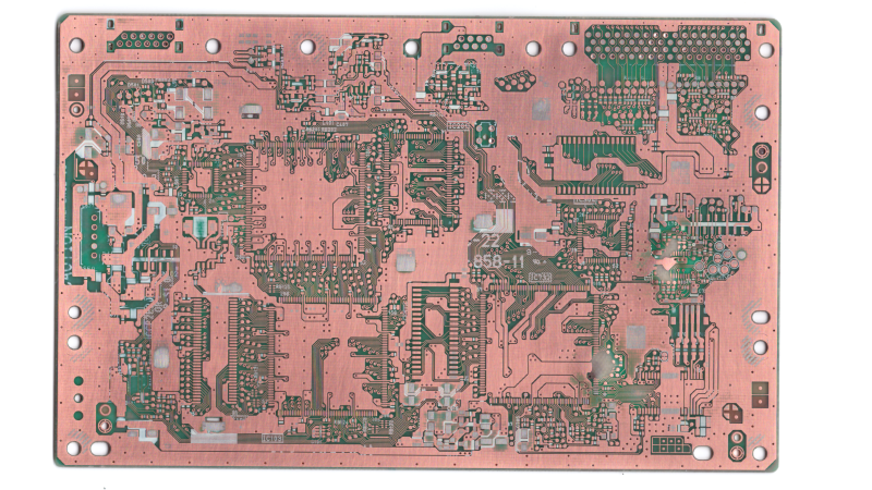
The first part of [Lawrence’s] quest was to try and reverse engineer the PlayStation motherboard itself. The 1990s console has the benefit of only using a two-layer PCB, meaning it’s far easier to trace out than more modern multi-layer designs. [Lawrence] started with a damaged console, pulled out the motherboard, and stripped off all the components. He then cleaned the board, scanned it, and then sandblasted it to remove the solder mask.
He’s begun the work of tracing out signals, and next on the agenda is to create a new custom PCB that’s compatible with the original PlayStation hardware. You can grab his work via GitHub if you’re interested. [Lawrence] is also excited about the possibilities of grabbing the 24-bit RGB signal heading into the GPU and using it for an HDMI output conversion in the future.
It’s always an exciting time in the PlayStation community; we see lots of great hacks on the regular. If you’re cooking up your own, don’t hesitate to drop us a line!












I remember seeing someone do this already in the past?
https://bitbuilt.net/forums/index.php?threads/an-attempt-to-recreate-the-ps2-pcb.4786/
Ooo neat. But no thats the PS2 this is the PS1.
True… Though I suppose a PS2 is also a PS1, no?
No, well, the ps1 is inside the ps2 as IO controller and in a special mode it runs ps1 code on the ps1 when playing a ps1 game. but no access to ps2 specific stuff. its embedded within the chipset
It would be interesting to pot more complex mainboards in a block of epoxy, then use a CNC machine, or a surface Grinder to shave off thin layers with a high resolution photo between each pass until you have successfully created a 3D stack of images of the entire PCB, from there use tools to extract a netlist of the whole board.
Surface grinder owners hate this one weird trick!
sand off the silkscreen and glue it to a piece of thick glass…more rigid and less wasteful…
but what would be 1000x better – modify a cheap pick and place or 3d printer into a flying lead tester, then go mildly insane on the software and presto – out comes a netlist.
Blind and buried vias kill that, and they’re much more common on complex boards in the past 5-10 years because the price has come down so much. Microvias are also much more common, which are exceptionally hard to probe. I’ve also had a few boards not even survive part removal.
For older stuff, though, sure. For those most of the detailed PCB design stuff (trace length matching, impedance control, etc.) was generally all massive overkill anyway, so reimplementing older stuff shouldn’t be that hard.
playstation was only a 2-layer PCB??? I can barely manage to route anything, let alone an entire game console, without 4 layers.
If OP wants a portal Playstation and also seeks good battery life, ditch the CD drive and look up SD based drive alternative like PSIO.
Even with the sony schematics and wiring board in a nice PDF, an actual CAD file you can alter might be way worth more. as a reference it might be usefull for some of us to know, the service manuals do contain some nice details and information https://www.psxdev.net/downloads/SCPH-100_5th-Edition.pdf
they also host the service manual for SCPH-7500 and SCPH-9000
Unfortunately SCPH-9000 service manual has a lot of errors in pilots.
It is much faster and easier to remove all the components and identify, creating a BOM, then sand the board down by hand (or with your choice of sander on a flat surface, or a surface grinder with a vacuum chuck, or a mill with a vacuum chuck, etc), scan each layer, import into a layout tool and align the layers, duplicate the layout (doesn’t have to be perfect if you are just going for a schematic), and create the netlist from the layout tool. You don’t even need to use a sanded image of the top and bottom layers if the copper is visible through the sildermask. All of the layout tools I’ve used support this method. You should be able to find all of the PCB footprints from the free EDA resources online which will save you some time in creating your netlist. Then from the netlist it is very easy to create a schematic. I’ve done this more times than I can count with up to 8 layer boards.
I can not imagine how much time it would take to try and draw a schematic by sitting there staring at the board and poking it with a multimeter, even for a 2 layer board of this size… My eyes and fingers would go numb…