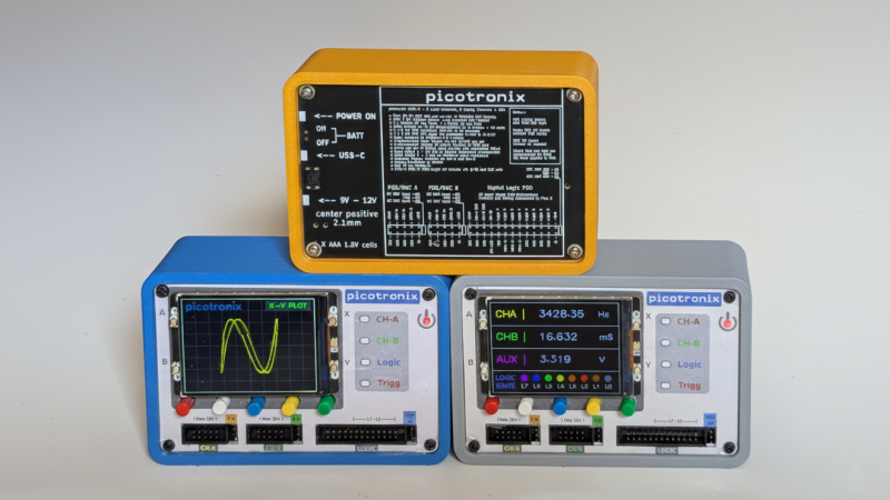
Hackers have been building their own basic oscilloscopes out of inexpensive MCUs and cheap LCD screens for some years now, but microcontrollers have recently become fast enough to actually make such ‘scopes useful. [NJJ], for example, used a pair of Raspberry Pi Picos to build Picotronix, an extensible combined oscilloscope and logic analyzer.
This isn’t an open-source project, but it is quite well-documented, and the general design logic and workings of the device are freely available. The main board holds two Picos, one for data sampling and one to handle control, display, and external communication. The control unit is made out of stacked PCBs surrounded by a 3D-printed housing; the pinout diagrams printed on the back panel are a helpful touch. One interesting technique was to use a trimmed length of clear 3D printer filament as a light pipe for an indicator LED.
Even the protocol used to communicate between the Picos is documented; the datagrams are rather reminiscent of Ethernet frames, and can originate either from one of the Picos or from a host computer. This lets the control board operate as an automatic testing station reporting data over a wireless or USB-connected network. The display module is therefore optional hardware, and a variety of other boards (called picoPods) can be connected to the Picotronix control board. These include a faster ADC, adapters for various analog input spans, a differential analog input probe, a 12-bit logic state analyzer, and a DAC for signal generation.
If this project inspired you to make your own, we’ve also seen other Pico-based oscilloscopes before, including one that used a phone for the display.


I feel like there is almost nothing a Pico can’t do, at least when it comes to matching tech from 1992 and earlier. it’s so great that all that capability is rolled up into a flexible $5 piece of tech. if it used a little less power, it would be a perfect target for my I2C slave code. but then again, i haven’t had luck putting i2c slave code on anything other than AVR 8-bit microcontrollers.
AI-generated make-believe images really don’t add anything to a post like this. If anything they just make me question if it’s just vaporware.
I don’t why they didn’t use just use renders, like some of the other pictures likely are. It would have felt less like a lie, since they should have all the parts if they can render it.
They later posted real pictures in another blog, but still never more than one.
What images are AI? The photos are all taken on a phone or camera.
The picture heading this post is AI. The smaller labels on the enclosures are AI gibberish.
For what it’s worth I had a good look through all the pictures and it does seem to be just that one. My guess is the physical product exists, but they wanted to show off some software features that don’t exist yet and made an AI edit
Thank you Skwid, this is John the other half of picotronix. I can assure you that every image on the site is real. Some of the original png images (most stored on the website server as well) are over a Mb. I compressed them using squoosh.app to webp, with a setting of around 75. Text detail will be lost with this setting. We wanted a site that loaded quickly. Feedback that this process makes the images look AI generated is a bit of a downer after 14 months hard work, but very useful.
We would hate to think that makers might be turned off a powerful test instrument targeted at their budgets, because a world saturated with AI imagery that make the non-existent look real, also leads us to believe the real is fake.
Once I iron out a few style bugs with Flarum, our Forum will be up for comments.
In response to the useful feedback here, I will try and get a Gallery page up tomorrow ( it is evening in QLD, Australia at present). I will provide the original high-res images, including traces of a signal at the input pin of the RP2350 ADC connected to both the picotronix and a Tektronix scope. We can also prove that we can subsample a periodic 10MHz signal (3dB attenuation) using the RP2350’s native 500kSPS ADC. Lots of pics.
BTW Jon H – well spotted on the enclosure labels, but they are not AI generated, they look like that because we did not want to use AI.
Production versions will be silk screened onto a Lexan panel. To provide something for a photo, Norm laser printed the panel onto (expensive) printable plastic from Office Works. Check out the hi-res pics on the forthcoming gallery, you may even see the imperfections where he has cut the holes with a scalpel for the buttons etc.
Please remember this is a real Kickstarter project with bumps that we are doing our best to eliminate along the way.
The header image that Jon H talked about, “https://picotronix.com/blog/wp-content/uploads/2025/11/picotronix-introduction.png”, has a lot of evidence of AI being used at some point. There is a lot of gibberish text, including “USS-C” instead of “USB-C” or “pasitive” instead of “positive”. The small text is completely incomprehensible. The readable text is still often arranged weird, like how each of the A’s in “AAA” is angled differently.
Also, this one is a PNG, so it wasn’t compressed. There’s no reason for it to look this way.
A compressed image like “https://picotronix.com/blog/wp-content/uploads/2026/01/case-back-blu.webp” has no such text distortions and is still readable. Everything is aligned correctly and even the smallest text resembles a valid word. Some of it might be hard to read, but I could decipher it with context.
They might have had only one completed device and used AI to make a picture of multiple. They have pictures of completed devices in the blog post, but I couldn’t find a real picture with multiple completed devices anywhere on the site, just pictures editted together or AI editted.
Hi Kevin
I have the original phone shot that the image was taken from – grey backing sheet allowed me to use gimp to do a perspective adjust, crop out the junk around the edges, then scale it down to 640×480. You can see that the display is identical – even the phase of the lissajous figure. Also, if you look at the front decals, the one on the left is not as clear as the other one (prototypes). On the website other photos have this same feature. The 3d Printed cases are also different.
https://i.postimg.cc/bJWSDg4R/PXL-20251104-020400340.jpg
Weirdly it almost matches this other image, which seems non-AI:
https://picotronix.com/blog/wp-content/uploads/2026/01/case-set-2.webp
So I think the header image is probably AI-upscaled for some reason.
I think people are so tired and suspicious of AI slop now that we ‘see’ it, whether it’s there, or not.
Why would they use AI when they clearly have the real thing (other photos clearly show genuine, readable text)? As far as I can see, the ‘suspicious’ image is just downscaled, or perhaps upscaled from a previously downscaled image. Either way, this looks real to me.
It is good to be suspicious, but I’d say it’s a real product due to the other images. These AI for upscale/downscale/small changes are muddying the water, and I don’t like it, but I get why these are favorable over learning basic image manipulation skills. It’s quick, it’s free, and it may even be good enough.
Hi Jan-Willem
I use gimp. Basic procedure is perspective, crop, background fill, and scale. Basic gimp skills that are pretty quick. It is the perspective, scaling and then compression that seems to distort images. I think that the heavy compression algorithms might be the culprit here. The compressors have to do a lot of tricks to get the images down, and maybe they are doing something that is like what the AI generators use. I am not sure as I don’t know a lot about how the AI image generation works.
Above, I posted the original from the phone – you can see that they are the same source. I doubt that there is any path to an AI image that can be faster than the simple gimp process. How would I get the basic information into the AI? Show it a photo of the real device? That can’t be a quick solution – it sounds like a nightmare.
https://i.postimg.cc/zDdTyp0Y/PXL-20250717-233615214.jpg
who knew AI liked pumpkins?
Yes, the labels on the left side of the front panel of the atop the stack in the lead photo don’t make sense if you read them. Also, the implied resolution is on the order of an iPhone Retina display, something which is not commonly available to the hobby market in that size at an affordable cost. My assessment is that it is AI malarkey, of which there is too much of these days.
All that aside, it would be neat to make a tiny instrument like that, but it would be difficult to use with a screen that tiny.
No – the display is 320×240 and it is a pimoroni Pico 2.8″ LCD designed to work with the Pico and pimoroni maintain an excellent graphics library. Their graphics library is written in C and is included in their 2350 micropython image. The library is quite similar to Raylib, without the 3d stuff. In fact, the 2.8″ display is very clear and bright, and (as you can see from the images), it can show nice waveforms. Look closer at the blog posts – you will see three running examples https://picotronix.com/blog/an-introduction-to-picotronix/.
But wait, these are not photos of the screen – AI shananagains! Because the Picographics is so similar to raylib, we wrote a Pyray wrapper that emulates the picographics library. That way we can drop the micropython code onto a PC python app and run it – so you can see what the pixels are doing. The simple app looks like this –
https://i.postimg.cc/sXCXbCTJ/pico-sim-640.jpg
The blog post about Picograms describes how the user interface can be migrated to a PC or external device. The data capture Pico 2 is effectively a server, so it gets a request message, collects data and sends it back via the data link. We don’t have fully user friendly PC software yet, but actually running the LCD software on a PC with the image scaled up would be a fairly easy option.
I mentioned this in another answer, but if you look closely, you will see simulated phosphor decay on one of the analog traces. The Pico 2 is capable of lots of drawing in a display cycle – which is 10-15 fps. The LCD is slow enough to not flicker, so it looks good. Note that the display Pico is mostly busy with the display, which is why we split the design into two parts – display, wifi and user interface, and signal processor. The signal processor is time critical and can’t be interrupted .
There is no “AI Malarkey” anywhere here. In fact, the only thing I find Chat useful for is looking up data sheets and general research help. I did use it to help write a polygon function, as raylib does not have a bitmap version. It did a good job there so that was a time saver.
def polygon(self, points):

    if len(points) < 3:

        return  # Need at least 3 points to form a polygon

    min_y = min(p[1] for p in points)

    max_y = max(p[1] for p in points)

    for y in range(min_y, max_y + 1):

        # Find intersections with this horizontal line

        intersections = []

        for i in range(len(points)):

            p1 = points[i]

            p2 = points[(i + 1) % len(points)]

            if (p1[1] <= y < p2[1]) or (p2[1] <= y < p1[1]):

                # Calculate intersection

                t = (y - p1[1]) / (p2[1] - p1[1])

                x = int(p1[0] + t * (p2[0] - p1[0]))

                intersections.append(x)

        # Sort and fill between pairs of intersections

        intersections.sort()

        for i in range(0, len(intersections), 2):

            if i + 1 < len(intersections):

                for x in range(intersections[i], intersections[i + 1]):

                    self.pixel(x, y)
That worked out of the box – so I was quite impressed with Chat for that little job.
Ah ha.
I was looking for the internal designs and details, but then I saw it.
This is a kickstarter project, so beyond the marketing rhetoric it’s all being kept secret by the creators to make money.
It’s just another Hackaday press release…
“This isn’t an open-source project, but it is quite well-documented, and the general design logic and workings of the device are freely available.”
I don’t really get the point of this, it is a not very good logic analyser and a pretty bad oscilloscope. I don’t see how 500 kSPS can use some DSP to reach an effective 10 MSPS and be useful in any way. They claim 100 MSPS on the logic analyser, they aren’t pushing data out over USB that fast or even to the display, that means it is stored in internal memory which isn’t all that large, even if they use external memory.
In my opinion something like the Analogy Discovery 3 would be much more useful and doesn’t need add ons to turn it into a waveform generator or a faster ADC.
Even other MCUs would make a better ADC. Some STM32 parts have ADCs up to 5 MSPS, support interleaving for higher speeds and have many more channels.
I think a cheaper or open source analog discovery 3 like device would be more useful. Especially with cheap logic analysers now.
Yeah the market is already saturated with surprisingly cheap scopes (USB and stand-alone) that have limited specs like this. I mean, imo the “bus pirate” already has the pico logic analyzer market locked up, and it seems like the bus pirate’s “just an afterthought” oscilloscope mode is comparable. And for just a little bit more money you can get an entry level “real scope” that has much better specs all around. Seems to me like just a neat demo project for the pico, not really a useful product.
The basic unit is designed to be entry level and cover the things that people who build with Electronics need. Scope, Logic capture, Metering. If you look closely at the demo screen with mixed signal, you will see that the LCD is doing phosphor decay emulation. Slow traces on scopes are really useful and you don’t need 1GS/s to do that. For many makers, students and Raspberry Pi users, utility trumps extreme performance. Simple add-ons that extend performance provide a way to grow into more specialized operations as required.
The Logic Analyser captures to internal memory, so that means only about 200K samples. It is not a stream to disk at USB3 speed – but neither is the AD3. Once its 32K internal buffer is full, it falls back to about 10MS/s (480Mb/s). Every design is subject to the same basic bandwidth constraints.
The picotronix logic trigger is implimented in PIO state machines, so they can be AND, OR and even sequential. The RP2350 is very versatile, and since we are targeting micropython, it is extensible. Once you understand the datagram protocol, anyone can write a custom server on the second Pico 2 module. The picotronix builds on the very well documented Raspberry Pi ecosystem. This is basically a different philosophy to the AD3 which is based around a Spartan FPGA – proprietary.
If you look at the pinouts for the Pod connectors, you can see that we provide access to many of the RP2350 GP ins and also the analog bus to the ADC pins. The logic Pod connector has 12 GP pins as well as power (+/5, 3.3) and an SPI/ser/i2c pair so it can get a plug in board to extend performance. Because that plugin is driven by state machines, it can be different functions. We have a Mixed Signal pcb that can interleave logic and a hi-speed ADC. Another one uses all 12 PIO pins to do a 12 ch Logic Analyzer. And another board uses the 12 GP signals to drive a R2R DAC. These are tools that might be useful to some people.
If you need to stream 10MS/s logic to a PC for several hours, or you are looking at 10nS rise times on a data line, you probably already have access to a high end scope and LA. The average user may not be so lucky.
I dont know what im looking at. No code, no diagrams, tiny screen and 5 buttons? But from whatever this is front page:
RP2350 state machines are clocked by default at 150MHz before any overclocking.
Practical limit is right there in RP2350 datasheet. “The six managers can access any six different crossbar ports simultaneously. So, at a system clock of 150 MHz, the
maximum sustained bus bandwidth is 3.6 GB/s”. Reading PIO with DMA consumes one port = 600MB/s at stock frequency with plenty of bandwidth left for other activities like writing it to ram, reading it back with another CPU core computing something, and finally pushing out thru SPI or SIO GPIO <- every stage gets its own AHB switch port with full separate dedicated 600MB/s.
One example of RP2350 LA sampling at 400Ms/s is https://github.com/gusmanb/logicanalyzer “This is an affordable logic analyzer capable of reaching up to 400Mhz of sampling speed. The analyzer uses a Pico/Pico2 as its core. The analyzer offers 24 channels but can be chained up to 5 devices allowing the sampling of up to 120 channels at once.”
Promise 10 or 100Mhz usable display, from 500K samples? No way.
100Mhz is the maximum sample rate of the MSO add-on module we have developed which uses the TI ADC08100. The Pico 2 cannot achieve a 100MHz clock, as its PIO max speed is 150MHz. There may be future Pico modules that go faster – we will see. The maximum sample rate at present is 75MHz, but the ADC we use is qualified for 100MHz. The ADC08100 has a bandwidth greater than 100MHz, but our analog chain is conservatively rated for 20MHz at 3Vpp.
Logic – the PIO state machines can sample the GP pins at 150MHz, but DMAing that to internal SRAM is constrained. We found that the fabric in the 2350 supports 32 bit transfers at up to 25MT/s. With the PIO serializers, this is 100MB/s. 5 bit Logic will work at 150MHz. For 8 bit logic, 50MS/s is safe and avoids fractional clock speeds.
The 10MHz figure refers to subsampled (ESR) captures using the 2350 ADC. The interesting thing here is that the RP2350 12 bit SAR is actually very good. The internal Sample and Hold and precise clocks allow some fancy DSP tricks. For DSP you need stable low jitter clocks, and the 2350 performs very well here.
The 2350 ADC is a typical SAR design that needs 2uS to complete a conversion. To do that, it has an inbuilt Sample and Hold that probably has an aperture of 10nS – 20nS. That value is then buffered and converted by the SAR logic over 2uS. The aperture grabs a snapshot of the voltage at the ADC pin, and this is divided by the capacitance tree.
There are two types of ESR – time domain and phase domain. Early Digital Tek scopes relied on a precise trigger, and then counted a delay to a sample (time domain). These samples were built up over many triggers to make a waveform. We use a phase technique where we measure the exact frequency of the wave, and then convert a set of samples into phase space, overlaying them on a reconstruction grid. The 2350 PIO makes frequency measurement possible with a “trigger” comparator on the analog channel driving a GP pin.
From measurements, the actual bandwidth (not sample rate) of the 2350 ADC seems to be just over 10MHz. After that the aperture window degrades the signal severely, and a sine wave mostly disappears at about 17MHz. The attached images show a 2.93MHz wave captured on a Tektroix scope at the adc pin, and the reconstructed wave. The ESR value is based on the wave period divided by the number of phase points captured. Only 97 samples were required. The 2350 is accurately replicating the applied wave – as you can see.
https://i.postimg.cc/fyj6wDsR/cap-2-93-tek.jpg
what the scope sees
https://i.postimg.cc/k43r5qz2/buff-offset-600.png
what the 2350 sees – it is not a sine, so the higher harmonics are being captured
https://i.postimg.cc/W1Ggynj1/esr-rf-10679.png
at 10MHz attenuation and distortion are beginning to cut in
Sub sampling of repeating waveforms is quite well understood. To manipulate sample in phase space you need some DSP and a floating point CPU. The 2350 has those things. ESR is not a single capture – it only looks at repeating waves like clocks and XTALs. One useful thing it can do is plot transfer functions of components like Op Amps – feed a square wave in and see what it looks like at the output. Keep in mind that until the 1GS/s scopes became common, repeating waveforms were all you could see on any scope.
Last sentence.
Analog storage scopes say ‘hi’.
Been looking at something related.
Hardware FIFOs are pretty cheap and give you a bunch of sRAM to hold samples.
You can throw money at the FIFO buffer and clock, to match your ADC spend.
In the end, I decided that I couldn’t hit a price point with todays ADCs and SOCs.
Yes point taken – analog storage scopes did exist, but they were pretty exotic. I think they stored the trace on the phosphor? I was going to mention them, but it would have taken quite a bit of explaining. Tektronix had all sorts of weird things, like dual timebases with delays on the second trace. I saw some of those old scopes and they looked a bit like a 747 cockpit control panel.
So, the cheapest way is probably to use some of the QSPI SRAM chips. Tricky to impliment, but better than FIFOs as they are now jelly bean devices.