Protel Autotrax is a PCB design tool first released for DOS in the mid-80s. Consider this a look at the history of PCB design software. I’m not recommending anyone actually use Protel Autotrax — better tools with better support exist. But it’s important to know where we came from to understand the EDA tools available now. I’m rolling up my sleeves (about 30 years worth of rolling) and building our standardized test PCB with the tool. Beyond this, I suggest viewing EEVblog #747, where [Dave] digs into one of his old project, Borland Pascal, and Protel Autotrax.
This is the continuation of a series of articles demonstrating how to Create A PCB In Everything. In this series, we take a standard reference circuit and PCB layout — a simple ATtiny85 board — and build it with different PCB design tools. We’ve already covered Eagle in this series. We learned Fritzing is a joke for PCB design, although it is quite good for making breadboard graphics of circuits. Each of these tutorials serves as a very quick introduction to a specific PCB design tool. Overall, this series provides for a comparison between different PCB design tools. Let’s dig into Protel Autotrax.
A short history of Protel, Altium, and Autotrax
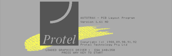
The company we know as Altium today was, for the first fifteen years of its existence, known as Protel. Back in the day, PCB design on a computer required a dedicated workstation, a lot of hardware, light pens, and everything was extraordinarily expensive. Protel was a reaction to this and the first product, Autotrax, was a DOS-based program that brought PCB design to the PC. A freeware version of Autotrax is still available on the Altium website and can be run from inside a DOS virtual machine or DOSBox.
Interestingly, Protel Autotrax is not the only PCB design software named Autotrax. A company called DEX 2020 has also has a PCB design software called AutoTRAX. This is weird, confusing, and I can’t figure out how this doesn’t violate a trademark. If anyone has any insight to what the Protel / Altium legal department was doing a few decades ago, your wisdom is welcome in the comments.
This week, we’re continuing our Creating A PCB In Everything series, where we go through the steps to create a simple, barebones PCB in different EDA suites. We’re done with Eagle, and now it’s time to move onto Fritzing.
Fritzing came out of the Interaction Design Lab at the University of Applied Sciences of Potsdam in 2007 as a project initiated by Professor Reto Wettach, André Knörig and Zach Eveland. It is frequently compared to Processing, Wiring, or Arduino in that it provides an easy way for artists, creatives, or ‘makers’ to dip their toes into the waters of PCB design.
I feel it is necessary to contextualize Fritzing in the space of ‘maker movement’, DIY electronics, and the last decade of Hackaday. Simply by virtue of being an editor for Hackaday, I have seen thousands of homebrew PCBs, and tens of thousands of amateur and hobbyist electronics projects. Despite what the Fritzing’s Wikipedia talk page claims, Fritzing is an important piece of software. The story of the ‘maker movement’ – however ill-defined that phrase is – cannot be told without mentioning Fritzing. It was the inspiration for CircuitLab, and the Fritzing influence can easily be seen in Autodesk’s 123D Circuits.
Just because a piece of software is important doesn’t mean it’s good. I am, perhaps, the world’s leading expert at assessing poorly designed and just plain shitty PCBs. You may scoff at this, but think about it: simply due to my vocation, I look at a lot of PCBs made by amateurs. EE professors, TAs, or Chris Gammell might beat me on volume, but they’re only looking at boards made by students using one tool. I see amateur boards built in every tool, and without exception, the worst are always designed in Fritzing. It should be unacceptable that I can even tell they’re designed in Fritzing.
Fritzing has its place, and that place is building graphical representations for breadboard circuits. Fritzing has no other equal in this respect, and for this purpose, it’s an excellent tool. You can also make a PCB in Fritzing, and here things aren’t as great. I want to do Fritzing for this Creating A PCB In Everything series only to demonstrate how bad PCB design can be.
For the next few thousand words, I am going to combine a tutorial for Fritzing with a review of Fritzing. Fritzing is an important piece of software, if only for being a great way to create graphics of breadboard circuits. As a PCB design tool, it’s lacking; creating parts from scratch is far too hard, and there’s no way to get around the grid snap tool. No one should ever be forced to create a PCB in Fritzing, but it does have its own very limited place.
For the next post in the Creating A PCB series, we’re going to continue our explorations of Eagle. In Part 1, I went over how to create a part from scratch in Eagle. In Part 2, we used this part to create the small example board from the Introduction.
This time around I’ll be going over Design Rule Check (DRC) — or making sure your board house can actually fabricate what you’ve designed. I’ll also be covering the creation of Gerber files (so you can get the PCB fabbed anywhere you want), and putting real art into the silkscreen and soldermask layers of your boards.
The idea behind this series is to explore different EDA suites and PCB design tools by designing the same circuit in each. You can check out the rest of the posts in this series right here.
In the last (and first) post in this series, we took a look at Eagle. Specifically, we learned how to create a custom part in Eagle. Our goal isn’t just to make our own parts in Eagle, we want to make schematics, boards, and eventually solder a few PCBs.
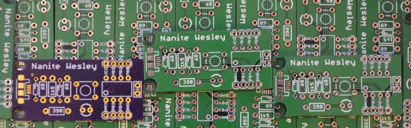
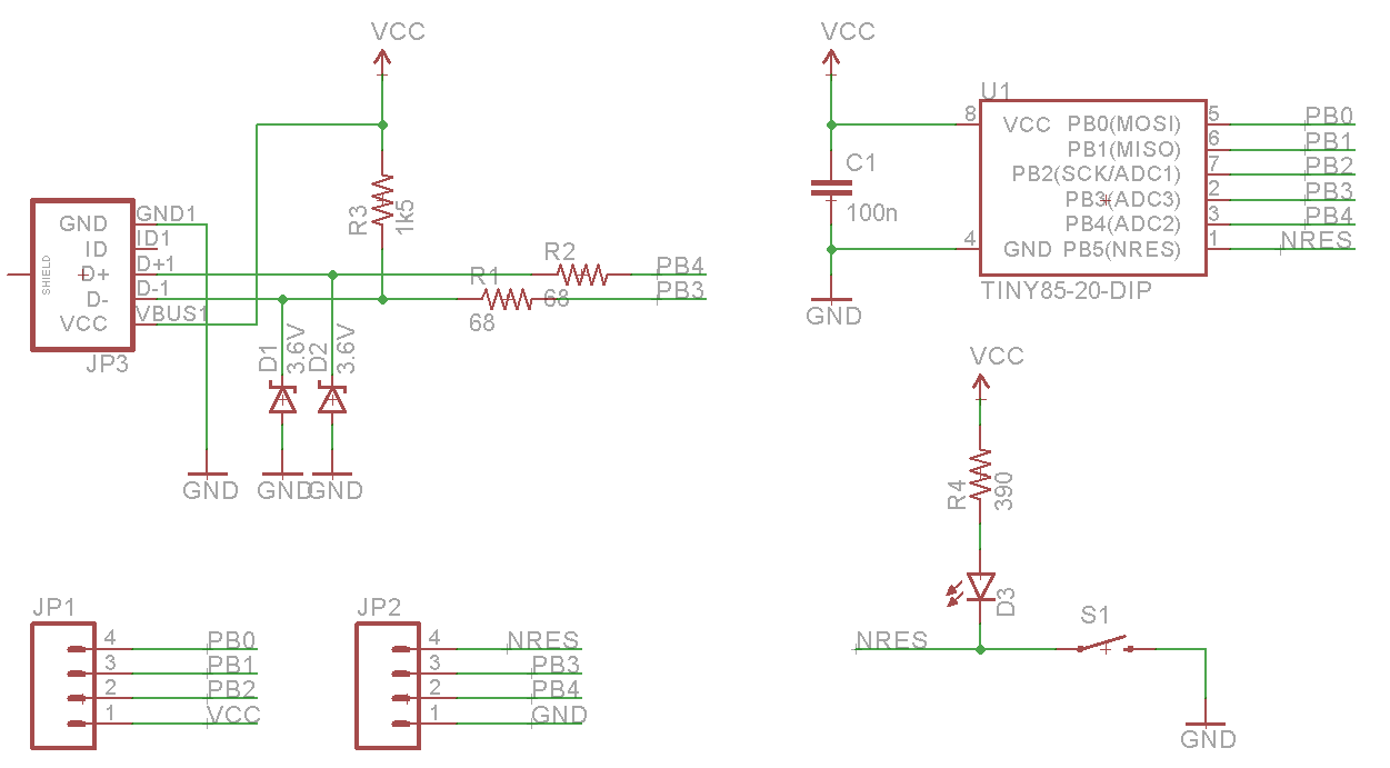
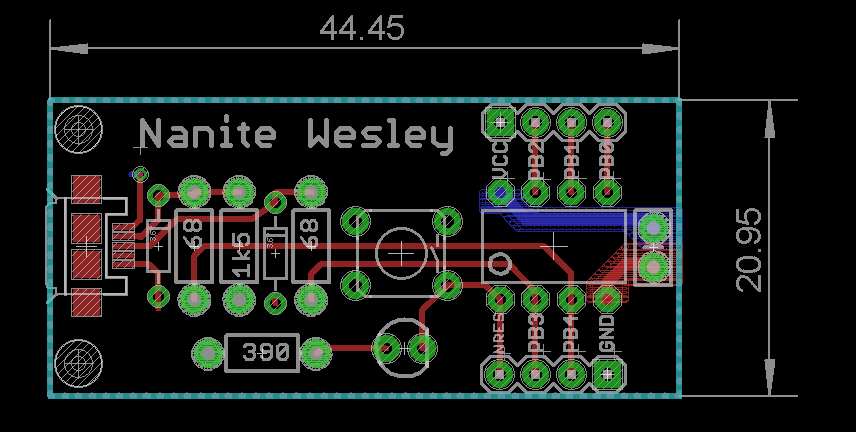
The board we’ll be making, like all of the boards made in this Creating A PCB In Everything series, is the Nanite Wesley, a small USB development platform based on the ATtiny85. This board has less than a dozen parts, most of which are through-hole. This is the simplest PCB I can imagine that has sufficient complexity to demonstrate how to make a board.
With that said, let’s get onto the second part of our Eagle tutorial and lay out our circuit board.
For the first in a series of posts describing how to make a PCB, we’re going with Eagle. Eagle CAD has been around since the days of DOS, and has received numerous updates over the years. Until KiCad started getting good a few years ago, Eagle CAD was the de facto standard PCB design software for hobbyist projects. Sparkfun uses it, Adafruit uses it, and Dangerous Prototypes uses it. The reason for Eagle’s dominance in a market where people don’t want to pay for software is the free, non-commercial and educational licenses. These free licenses give you the ability to build a board big enough and complex enough for 90% of hobbyist projects.
Of course, it should be mentioned that Eagle was recently acquired by Autodesk. The free licenses will remain, and right now, it seems obvious Eagle will become Autodesk’s pro-level circuit and board design software.
Personally, I learned PCB design on Eagle. After a few years, I quickly learned how limited even the professional version of Eagle was. At that point, the only option was to learn KiCad. Now that Eagle is in the hands of Autodesk, and I am very confident Eagle is about to get really, really good, I no longer have the desire to learn KiCad.
With the introduction out of the way, let’s get down to making a PCB in Eagle.
A few years ago, I wrote a few columns titled Making A Thing. These columns were a tutorial of sorts for several different 3D modeling programs. This column wasn’t meant to be a complete guide to modeling an object in OpenSCAD or SolidWorks, it was just step-by-step instructions on how to make one specific thing with one specific piece of software.
More than a few people in the Hackaday community found this column useful or at the very least an interesting pedagogical device. When starting out with any kind of productivity software, you don’t need to know how to do everything, you just need to know how to do the most common tasks.
Since the Making A Thing column was so popular, I felt it was time to revive this idea with another design task we often face. As you have already guessed, we’re going to be making printed circuit boards. Continuing the unique tutorial format created in the previous iteration of this column, Making a PCB will build one specific circuit in multiple EDA suites.
The Circuit
The entire concept of demonstrating how to build one thing in a specific software package necessitates a model thing. Before I even begin writing the first Making A PCB column, I need to design something that’s sufficiently complex but still relatively simple, and something that’s hopefully somewhat useful. Breakout boards are extremely simple, perhaps too much. In the course of these programs, I’ll need to demonstrate how to make a part in each specific software suite, so fewer pins are better.
Lacking any creativity of my own, I’ve settled on a very small ATtiny85 Arduino derivative from Tim a.k.a. [cpldcpu]. Tim’s Nanite 85 is an exceptionally small Arduino-compatible board based on the ATtiny85, complete with a USB port, LED, and a few pins of I/O. It’s simple but sufficiently complex to give an introduction to a PCB design suite.
I’m not going to outright copy Tim’s Nanite 85, though. It’s much clearer if parts aren’t stacked on top of each other, and I’d like to give myself a little breathing room on the layout. I’ve redesigned the circuit of the Nanite 85 to use mostly through-hole parts on a slightly larger board. I’m calling my version the Nanite Wesley, and if you get that reference, thumbs up for you.
The schematic for the Nanite WesleyThe Nanite Wesley board. Copper pours not shown
Is this how a board should be laid out? No, absolutely not. I could probably do this as a single-layer board. This is a very inefficient layout, and I like rounded corners on my boards. It’s good enough, though, and it works. This is meant to be a tutorial on how to use a PCB design package, not a tutorial on how to design a PCB. Your criticisms in this regard are noted and ignored.
What These Tutorials Will Consist Of
You cannot use a PCB design package until you know how to make a part. Yes, Eagle has wonderful libraries for almost everything you can imagine, KiCad has plenty of parts on the Internet, and if you’re using a cloud-based PCB software, almost everything will be provided for you. If you make a PCB, eventually you’ll have to make your own part, though, and each tutorial will begin with making a DIP-8 ATtiny85. Everything else on this board is a jellybean part. Either way, the process of making a part and package for a Zener is the same as making one for a microcontroller.
The next part of the tutorial will consist of schematic capture. This means placing the parts in the schematic, drawing wires between the pins and pads, and naming them. From there, it’s time to actually make a board, and this means dropping the parts down, putting traces between all the pins, doing the board outline, pouring copper, and mechanical considerations.
With the schematic and board designed, it will be time to send it off to a fab house. For Eagle and KiCad, this is easy; OSHpark accepts Eagle .brd and KiCad .pcb files, but this is cheating. We’re going to use CAM to generate real Gerber files. If you make enough PCBs, you’ll have to learn it eventually.
Caveats and Poor Design
There are a lot of things that go into making a ‘proper’ PCB, including isolation, direct traces to decoupling capacitors, making sure pixies don’t go around sharp corners and a thousand other items that won’t be discussed in these tutorials. There’s a reason I won’t be discussing this. This is a guide on how to use a PCB design tool, not how to design a PCB.
What else should I do?
As you can probably guess from the schematic above, the first PCB software I’m going to cover is Eagle. KiCad is on the list, as is Fritzing, Altium CircuitMaker, and OrCAD. In the interests of putting PCB design in a historical context, I have a copy of AutoTRAX and an old DOS machine. I’ll also be covering a few of the cloud-only design tools such as Upverter.
That’s enough software suites to get started, but as with the Making A Thing series, I’m going to be looking for suggestions from the peanut gallery. I can’t change the circuit I’m making, as that’s the entire point of this series, but I am looking for suggestions on other tools to cover. What else can I do? Want me to grab a piece of copper clad board, sticker overlays, and some photostatic film? I can do that. Are you at a web-based EDA startup, and want some free advertising? Leave a note in the comments.
Thanks to our efforts to slowly improve the backend of Hackaday, you’ll be able to access all the Making A PCB In Everything posts from the series list below.