Do you do PCB design for a living? Has KiCad been just a tiny bit insufficient for your lightning-fast board routing demands? We’ve just been graced with the KiCad 9 release (blog post, there’s a FOSDEM talk too), and it brings features of the rank you expect from a professional-level monthly-subscription PCB design suite.
Of course, KiCad 9 has delivered a ton of polish and features for all sorts of PCB design, so everyone will have some fun new additions to work with – but if you live and breathe PCB track routing, this release is especially for you.
A few days ago, KiCad 8 was released, and it’s a straight upgrade to any PCB designer’s quality of life. There’s a blog post as usual, and, this year, there’s also a FOSDEM talk from [Wayne Stambaugh] talking about the changes that we now all get to benefit from. Having gone through both of these, our impression is that KiCad 8 developers went over the entire suite, asking: “this is cool, but could we make it better”? The end result is indeed a massive improvement in a thousand different ways, from small to fundamental, and all of them seem to be direct upgrades from the KiCad 7 experience.
Yesterday, the KiCad team has released KiCad 7.0.0 – a surprise for those of us who have only gotten used to the wonders of KiCad 6, and it’s undoubtedly a welcome one! Some of these features, you might’ve seen mentioned in the KiCad 2022 end-of-year recap, and now, we get to play with them in a more stable configuration. There’s a trove of features and fixes for all levels of KiCad users, beginners, hobbyists and professionals alike – let’s start with some that everyone can appreciate! Continue reading “KiCad 7.0.0 Is Here, Brings Trove Of Improvements”→
[Chris Gammell] moderated the KiCad 2022 End-of-Year Recap with several KiCad developers and librarians. They reviewed what’s been bubbling up in the nightly KiCad 6 builds, what we can expect from KiCad 7, and even answered some questions from the user community. Over the course of 2022, the KiCad project has grown both its development team and library team. The project even has a preliminary support commitment from the CERN Drawing Office!
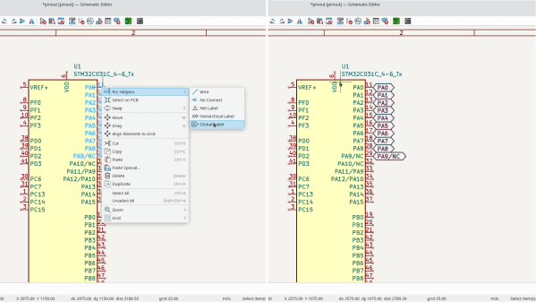
Improvements to the KiCad Schematic Editor include smart wire dragging that simplifies moving components around within schematic diagrams. Components selected in the schematic now remain selected while switching to the PCB Editor. Internal documentation of schematics has advanced with support for fonts, embedded graphics, and the inclusion of hypertext links to datasheets and other reference materials. New features for PDF generation offer interactive files and links between sheets.
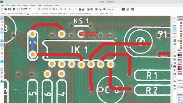
A new search panel within the KiCad PCB Editor supports finding components by footprint, net, or text search. A property panel allows common properties to be edited across multiple selected items. While a full-blown auto-router remains outside of the scope for KiCad, “push and shove” routing is faster and easier. An “attempt to finish” feature routes a quick connection for the currently selected trace, and “pack and move” positions all selected footprints into proximity to simplify placing them as neighbors within the board layout.
The KiCad PCB Editor also adds support for the use of fonts and inverted “knockout text” which even works on copper zones. Bitmap graphics can be imported and scaled beneath layout work as reference illustrations. Private footprint layers can be used to place extra documentation within footprints. The design rule checker (DRC) now can catch more layout issues, especially those that may impact manufacturability.
These are just a sampling of the impressive improvements we can expect with KiCad 7.0. There are also additions to circuit simulation and modeling features, a new command line interface for script-based automation, ARM64 support for KiCad running on Apple silicon, and a huge number of additions to the default library including symbols, footprints, and 3D Viewer models.
The KiCad team suggests several ways to support the project. There are always needs for additional developers and librarians. Financial contributions can be made at kicad.org. As users, we can run the nightly builds, try to break them, and give feedback in the form of detailed bug reports. Community testing will help make KiCad 7.0 as solid as possible. The project team is also seeking open hardware projects to include with KiCad 7.0 as demos. For example, the StickHub project was included with KiCad 6.0 as a demo.
The official release of KiCad 7.0 is currently scheduled for January 31, 2023. While we wait, let’s flashback to our January 2022 presentation of what features made it into the KiCad 6.0 release.
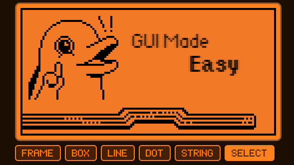
[Mikhail] released a handy GUI editor/generator tool for the Flipper Zero multipurpose hacker tool, making layouts and UI elements much easier and more intuitive to craft up.
Those who decide to delve into rolling their own applications or add-ons will find this a handy resource, especially as it generates the necessary code for the visual elements. It’s not limited to placing icons, either. Boxes, lines, dots, text, and more can be freely laid out to get things looking just right.
To use it, simply drag and drop icons of various sizes into the screen area. Non-icon UI elements like frames, lines, text, and others can be placed with a click using the buttons. To move elements around, click the SELECT button first, then drag things as needed. To fine-tune positioning (or change the text of a string) a selected element’s properties can be accessed and modified to the right of the simulated screen. When things look good, switch to the CODE tab and copy away to use it in your Flipper application.
Unfamiliar with the Flipper Zero? It’s a kind of wireless multitool; a deeply interesting device intended to make wireless exploration and experimentation as accessible as its dolphin mascot is adorable.
A few years ago, I wrote a few columns titled Making A Thing. These columns were a tutorial of sorts for several different 3D modeling programs. This column wasn’t meant to be a complete guide to modeling an object in OpenSCAD or SolidWorks, it was just step-by-step instructions on how to make one specific thing with one specific piece of software.
More than a few people in the Hackaday community found this column useful or at the very least an interesting pedagogical device. When starting out with any kind of productivity software, you don’t need to know how to do everything, you just need to know how to do the most common tasks.
Since the Making A Thing column was so popular, I felt it was time to revive this idea with another design task we often face. As you have already guessed, we’re going to be making printed circuit boards. Continuing the unique tutorial format created in the previous iteration of this column, Making a PCB will build one specific circuit in multiple EDA suites.
The Circuit
The entire concept of demonstrating how to build one thing in a specific software package necessitates a model thing. Before I even begin writing the first Making A PCB column, I need to design something that’s sufficiently complex but still relatively simple, and something that’s hopefully somewhat useful. Breakout boards are extremely simple, perhaps too much. In the course of these programs, I’ll need to demonstrate how to make a part in each specific software suite, so fewer pins are better.
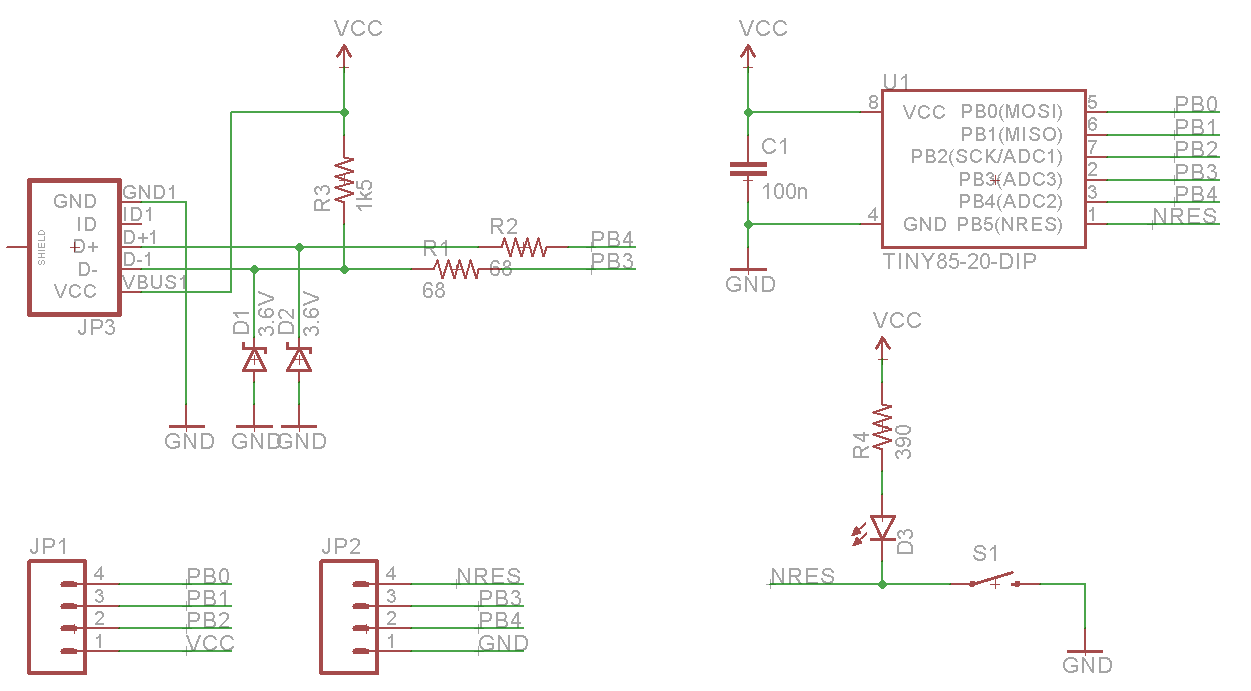
Lacking any creativity of my own, I’ve settled on a very small ATtiny85 Arduino derivative from Tim a.k.a. [cpldcpu]. Tim’s Nanite 85 is an exceptionally small Arduino-compatible board based on the ATtiny85, complete with a USB port, LED, and a few pins of I/O. It’s simple but sufficiently complex to give an introduction to a PCB design suite.
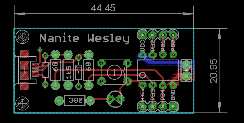
I’m not going to outright copy Tim’s Nanite 85, though. It’s much clearer if parts aren’t stacked on top of each other, and I’d like to give myself a little breathing room on the layout. I’ve redesigned the circuit of the Nanite 85 to use mostly through-hole parts on a slightly larger board. I’m calling my version the Nanite Wesley, and if you get that reference, thumbs up for you.
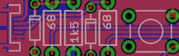
The schematic for the Nanite WesleyThe Nanite Wesley board. Copper pours not shown
Is this how a board should be laid out? No, absolutely not. I could probably do this as a single-layer board. This is a very inefficient layout, and I like rounded corners on my boards. It’s good enough, though, and it works. This is meant to be a tutorial on how to use a PCB design package, not a tutorial on how to design a PCB. Your criticisms in this regard are noted and ignored.
What These Tutorials Will Consist Of
You cannot use a PCB design package until you know how to make a part. Yes, Eagle has wonderful libraries for almost everything you can imagine, KiCad has plenty of parts on the Internet, and if you’re using a cloud-based PCB software, almost everything will be provided for you. If you make a PCB, eventually you’ll have to make your own part, though, and each tutorial will begin with making a DIP-8 ATtiny85. Everything else on this board is a jellybean part. Either way, the process of making a part and package for a Zener is the same as making one for a microcontroller.
The next part of the tutorial will consist of schematic capture. This means placing the parts in the schematic, drawing wires between the pins and pads, and naming them. From there, it’s time to actually make a board, and this means dropping the parts down, putting traces between all the pins, doing the board outline, pouring copper, and mechanical considerations.
With the schematic and board designed, it will be time to send it off to a fab house. For Eagle and KiCad, this is easy; OSHpark accepts Eagle .brd and KiCad .pcb files, but this is cheating. We’re going to use CAM to generate real Gerber files. If you make enough PCBs, you’ll have to learn it eventually.
Caveats and Poor Design
There are a lot of things that go into making a ‘proper’ PCB, including isolation, direct traces to decoupling capacitors, making sure pixies don’t go around sharp corners and a thousand other items that won’t be discussed in these tutorials. There’s a reason I won’t be discussing this. This is a guide on how to use a PCB design tool, not how to design a PCB.
What else should I do?
As you can probably guess from the schematic above, the first PCB software I’m going to cover is Eagle. KiCad is on the list, as is Fritzing, Altium CircuitMaker, and OrCAD. In the interests of putting PCB design in a historical context, I have a copy of AutoTRAX and an old DOS machine. I’ll also be covering a few of the cloud-only design tools such as Upverter.
That’s enough software suites to get started, but as with the Making A Thing series, I’m going to be looking for suggestions from the peanut gallery. I can’t change the circuit I’m making, as that’s the entire point of this series, but I am looking for suggestions on other tools to cover. What else can I do? Want me to grab a piece of copper clad board, sticker overlays, and some photostatic film? I can do that. Are you at a web-based EDA startup, and want some free advertising? Leave a note in the comments.
Thanks to our efforts to slowly improve the backend of Hackaday, you’ll be able to access all the Making A PCB In Everything posts from the series list below.