New Bismuth Transistor Runs 40% Faster And Uses 10% Less Power

Recently in material science news from China we hear that [Hailin Peng] and his team at Peking University just made the world’s fastest transistor and it’s not made of silicon. Before we tell you about this transistor made from bismuth here’s a whirlwind tour of the history of the transistor.

The Bipolar Junction Transistor (BJT, such as NPN and PNP) was developed soon after the point-contact transistor which was developed at Bell Labs in 1947. Then after Resistor-Transistor Logic (RTL) came Transistor-Transistor Logic (TTL) made with BJTs. The problem with TTL was too much power consumption.

Continue reading “New Bismuth Transistor Runs 40% Faster And Uses 10% Less Power”

Intel Says Nanowire And NanoRibbon In Volume In Five Years

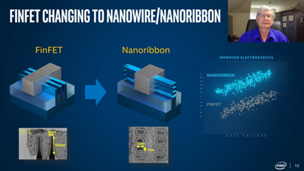
Intel’s CTO says the company will eventually abandon CMOS technology that has been a staple of IC fabrication for decades. The replacement? Nanowire and nanoribbon structures. In traditional IC fabrication, FETs form by doping a portion of the silicon die and then depositing a gate structure on top of an insulating layer parallel to the surface of the die. FinFET structures started appearing about a decade ago, in which the transistor channel rises above the die surface and the gate wraps around these raised “fins.” These transistors are faster and have a higher current capacity than comparable CMOS devices.

However, the pressure of producing more and more sophisticated ICs will drive the move away from even the FinFET. By creating the channel in multiple flat sheets or multiple wires the gate can surround the channel on all sides leading to even better performance. It also allows finer tuning of the transistor characteristics.

Continue reading “Intel Says Nanowire And NanoRibbon In Volume In Five Years”