[Jan Mrázek] is a pro when it comes to rolling his own PCBs. He can crank out a 6/6 mil double-sided PCB in 45 minutes flat. As a challenge to his prowess, he decided to experiment with plating through-hole PCBs at home, because sometimes you just can’t wait for China to deliver the goods.
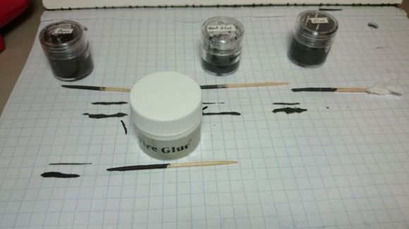
The key here is to make a non-conductive surface—the walls of holes drilled in a sheet of copper clad–conductive. While there are some established ways of doing this at home, the chemicals are difficult to source. When his local supplier started stocking colloidal graphite paint, which is used to prevent ESD and fix non-working remote control buttons, he decided to try it.
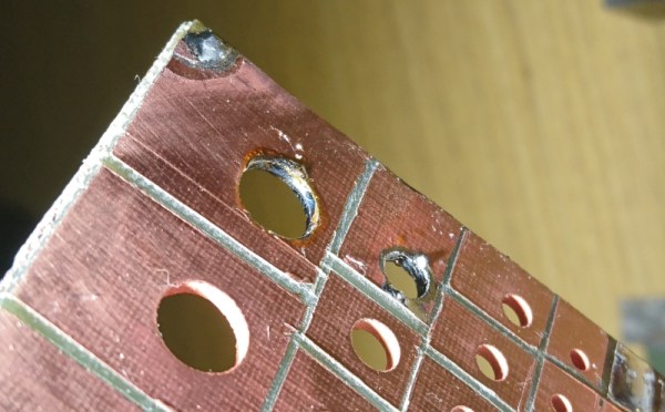
[Jan] drilled up a board with holes ranging from 0.1mm up to 8mm, polished it, and gave it an acetone bath. He sprayed each side with graphite and cured it at 100 °C for 20 minutes. At this point, wall hole resistance measured 21 Ω. [Jan] wet-sanded away the graphite and set up an electroplating bath. Right away, he could see a layer of copper forming on the holes. After 90 minutes, he polished the board again and separated the vias to prepare for the real test: solder. This time, every hole except the smallest size reported a resistance of 0.1 Ω. But they all sucked solder through the vias, making this experiment a success.
[Jan] concluded that this is a simple and effective process, but is rarely worth the effort. We wonder how the simplicity of this method compares to drilling wells instead of holes, filling them with conductive ink, and then drilling the rest of the via.
Via [Dangerous Prototypes]


