Nintendo DSi Teardown

dsi_teardown

[bunnie] managed to pick up a Nintendo DSi while in Japan. It seems he had the device running less than an hour before he tore it down for an impromptu hotel photoshoot. There’s nothing too surprising and he mentions that the CPU certainly feels more capable than the previous model, which may explain the shorter battery life. The ARM processor sits under an RF shield directly below the WiFi card. The best photo is the top side of the board with every single debug point labeled in plain English on the silkscreen. We’re sure that’ll help with the development of new homebrew hardware.

[bunnie] has posted some interesting teardowns in the past. Have a look at his Sony XEL-1 teardown to see the inner workings of an OLED TV.

Sony XEL-1 OLED Teardown


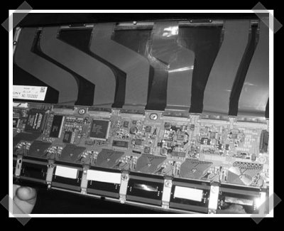
[bunnie] just happened to be at the Embedded Systems Conference in San Jose on exactly the right day to witness the live teardown of a Sony XEL-1 OLED TV. The XEL-1 is Sony’s flagship OLED panel that’s only 3mm thick… and $2500 for just an 11-inch screen. [bunnie] was able to take quite a few shots of the components as they were passed around. He pointed out a few interesting bits about the construction. There seems to be quite a bit of thermal material on the display to prevent “avalanche thermal failures” (which I’m guessing doesn’t look as cool as it sounds). OLED displays are completely transparent and their legendary contrast ratio is just a result of the dark backing material. The mainboard seems to be a bit of overkill for this TV and [bunnie] concludes that it’s just the standard image engine architecture from Sony’s Bravia line put into a smaller package.