A normal life in hacking, if there is such a thing, seems to follow a predictable trajectory, at least in terms of the physical space it occupies. We generally start small, working on a few simple projects on the kitchen table, or if we start young enough, perhaps on a desk in our childhood bedroom. Time passes, our skills increase, and with them the need for space. Soon we’re claiming an unused room or a corner of the basement. Skills build on skills, gear accumulates, and before you know it, the garage is no longer a place for cars but a place for pushing back the darkness of our own ignorance and expanding our horizons into parts unknown.
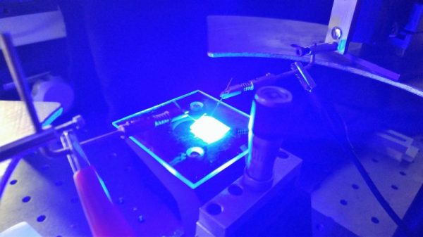
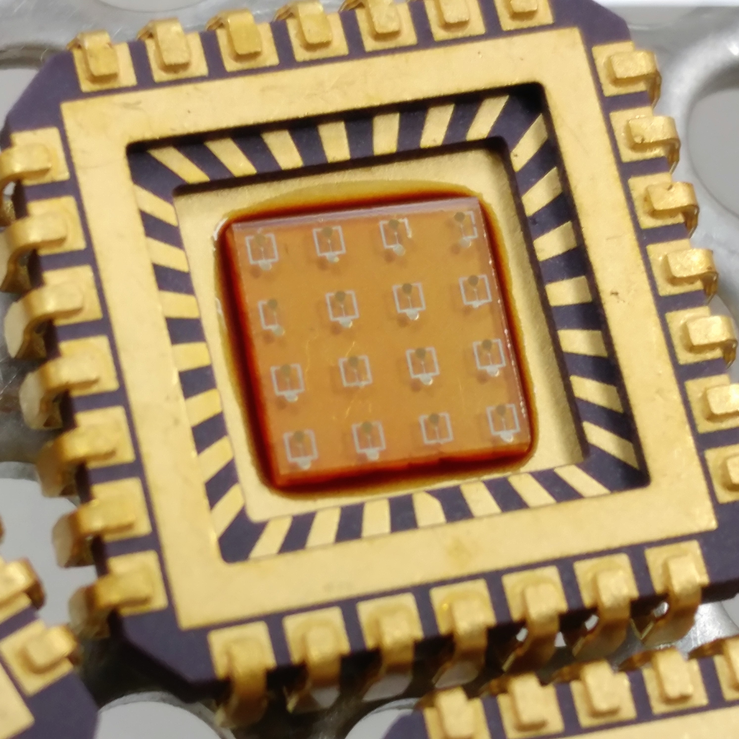
It appears that Sam Zeloof’s annexation of the family garage occurred fairly early in life, and to a level that’s hard to comprehend. Sam seems to have caught the hacking bug early, and by the time high school rolled around, he was building out a remarkably well-equipped semiconductor fabrication lab at home. Sam has been posting his progress regularly on his own blog and on Twitter, and he dropped by the 2018 Superconference to give everyone a lesson on semiconductor physics and how he became the first hobbyist to produce an integrated circuit using lithographic processes.
Continue reading “Of Roach Killer And Rust Remover: Sam Zeloof’s Garage-Made Chips”