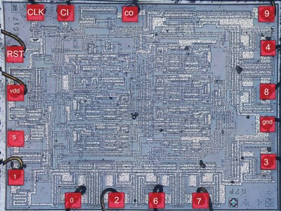
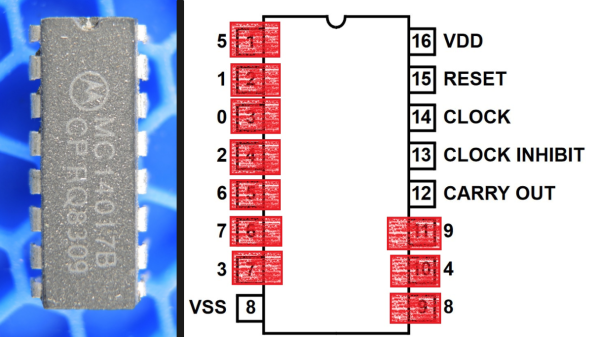
If you’ve ever handled a chip with a really strange or highly inconvenient pinout and suspected that the reason had something to do with the inner workings, you may be interested to see [electronupdate]’s analysis of why the 4017 Decade Counter IC has such a weirdly nonintuitive pinout. It peeks into an IC design dating from the 1970s to see an example of the kind of design issues that can affect physical layout.

In the case of the 4017, once decapped and the inner workings exposed, things became more clear. Inside the chip are a bunch of flip-flops and NAND gates, laid out in a single layer. Some of the outputs (outputs 5 and 1 for example, physically on pins 1 and 2 respectively) share the same flip-flop.
The original design placed the elements in a way that made the most logical sense for routing and layout, which resulted in nice and tidy inner workings but an apparently illogical pinout. A lot of this is probably feeling familiar to anyone who has designed and routed a single-layer PCB, where being limited to one layer makes it important to get the most connections as directly near one another as possible.
Chip design has of course come a long way since the 70s, but there is forever some level of trade-off to be made between outward tidiness and inner design harmony. The next time you’re looking at a part with an apparently illogical pinout, there’s a fair chance it makes far more sense on the inside.
If any of you are interested in decapping ICs yourselves to see what’s inside, we saw that it’s possible with commonly available chemicals, not just nasty ones.


