Four square, unpopulated purple PCBs sit in front of a tube of soldering flux on a light grey work surface. The PCBs are only 1"x1".

BeagleStamp Makes Soldering Linux Into Your Projects Easier

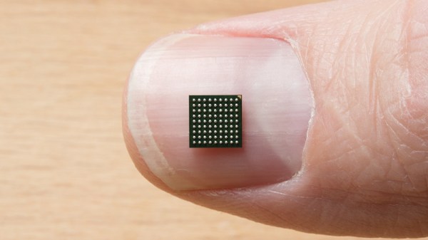
There are a lot of things you can do with today’s powerful microcontrollers, but sometimes you really need a full embedded Linux setup. [Dylan Brophy] wanted to make it easier to add Linux to his own projects and designed the BeagleStamp.

A populated purple PCB propped against a piece of wood on a light grey work surface. The bulk of the PCB is covered in an Ocatavo processor chip.
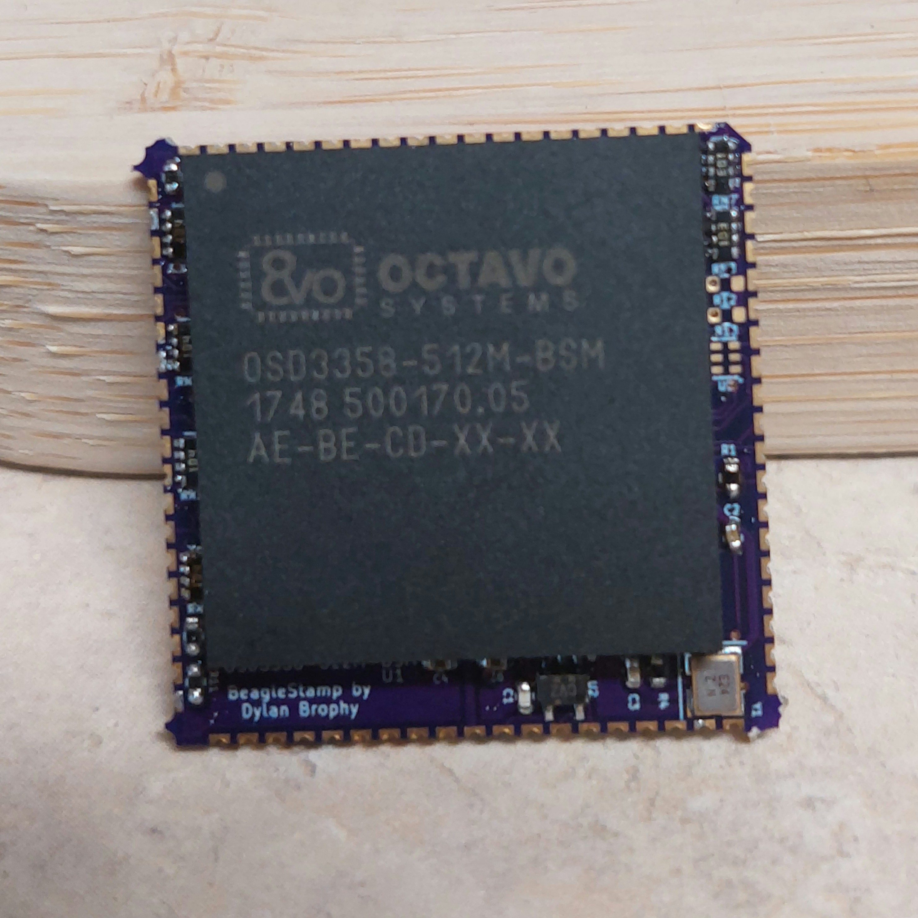
Squeezed onto a 1″ square, the BeagleStamp puts the power of a PocketBeagle into an easy to solder module you can add to a project without all that tedious mucking about with individually soldering all the components of a tiny Linux computer every time. As a bonus, the 4 layer connections are constrained to the stamp as well, so you can use lower layer count boards in your project and have your Linux too.

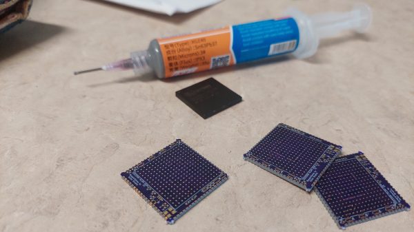
The first run of boards was delivered with many of the pins unplated, but [Brophy] plans to work around it for the time being so he can spot any other bugs before the next board revision. Might we suggest a future version using RISC-V?

How To Design A BGA Breakout Module

Surface mount devices can take some adjusting to for hackers primarily used to working with through-hole components. Despite this, the lure of the hottest new parts has enticed even the most reticent to learn to work with the technology. Of course, time rolls on and BGA parts bring further difficulties. [Nate] from SparkFun worked on the development of the RedBoard Artemis, and broke down the challenges involved.

The RedBoard Artemis is an Arduino-compatible devboard built around the Ambiq Apollo3 chip. In addition to packing Bluetooth and 1 MB of Flash, it’s also capable of running TensorFlow models and using tiny amounts of power. The chip comes in an 81-Ball Grid Array at 0.5mm pitch, which meant SparkFun’s usual PCB fabrication methods weren’t going to cut it.

An initial run of prototype boards was run using 4 layers, blind and buried vias, and other fancy tricks to break out all the necessary signals. While this worked well, it was expensive and inefficient. The only part of the board that needed such fabrication was around the chip itself; the rest of the board could be produced with cheaper 2-layer methods. To improve this for mass production, instead, an SMD module was created to house the Apollo3, which could then be dropped into new designs on cheaper boards as necessary.

[Nate] does a great job of explaining the engineering involved, as well as sharing useful tips for others going down a similar path. So far, this is just part 1, with future posts promising to cover the RF shield design and FCC certification process. [Nate] has always been keen to share his wisdom, and we can’t wait to see what comes next!