How do you clean the residual flux off your boards? There are plenty of ways to go about the job, ranging from “why bother?” to the careful application of isopropyl alcohol to every joint with a cotton swab. It seems like more and more people are turning to ultrasonic cleaners to get the job done, though, and for good reason: just dunk your board and walk away while cavitation does the work for you.
But just how safe is it to sonically blast the flux off your boards? [SDG Electronics] wanted to know, so he ran some cleaning tests to get to the bottom of things. On the face of it, dunking a PCB in an aqueous cleaning solution seems ill-advised; after all, water and electricity famously don’t mix. But assuming all the nooks and crannies of a board can be dried out before power is applied, the cleaning solution itself should be of little concern. The main beef with ultrasonic cleaning seems to be with the acoustic energy coupling with mechanical systems on boards, such as crystal oscillators or micro-electrical-mechanical systems (MEMS) components, such as accelerometers or microphones. Such components could resonate with the ultrasonic waves and be blasted to bits internally.
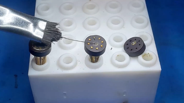
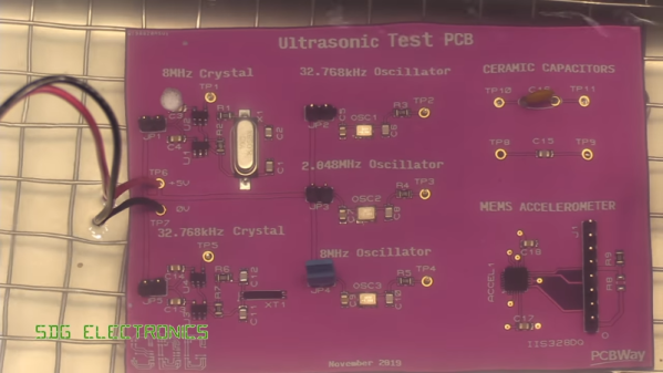
To test this, [SDG Electronics] built a board with various potentially vulnerable components, including the popular 32.768-kHz crystal, cut for a frequency quite close to the cleaner’s fundamental. The video below goes into some detail on the before-and-after tests, but the short story is that nothing untoward happened to any of the test circuits. Granted, no components with openings as you might find on some MEMS microphones were tested, so be careful. After all, we know that ultrasound can deal damage, and if it can levitate tiny styrofoam balls, it might just do your circuit in.
Continue reading “How Safe Is That Ultrasonic Bath For Flux Removal?”