The idea of trying to prototype with SMD parts on the fly sounds like insanity, right? But then we watched [Leo Fernekes] walk calmly and carefully through his process (video, embedded below). Suddenly, SMD prototyping jumped onto our list of things to try soon.
[Leo] speaks from a lot of experience and tight client timelines, so this video is a fourteen-minute masterclass in using copper-clad board as a Manhattan-style scratch pad. He starts by making a renewable tool for scraping away copper by grinding down and shaping an old X-Acto blade into a kind of sharpened Swiss Army knife bottle opener shape. That alone is mind-blowing, but [Leo] keeps on going.
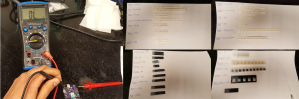
 In these prototypes, he uses the through-hole version of whatever microcontroller is in the design. For everything else, he uses the exact SMT part that will end up on the PCB that someone else is busy designing in the meantime.
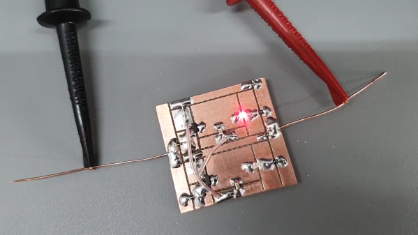
After laying the board out on paper, [Leo] carves out the islands of conductivity, beep-checks them for shorts, shines the whole thing with steel wool, and goes to town.
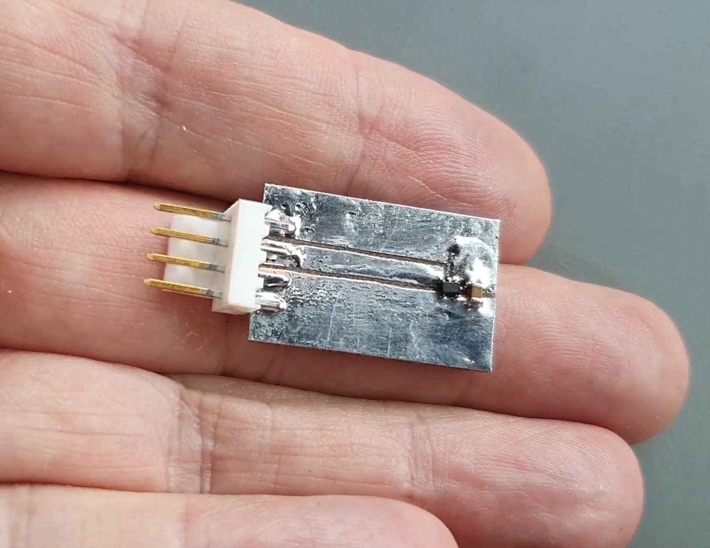
The tips and tricks keep coming as he makes jumps and joins ground planes with bare copper wire insulated with heat-proof Teflon tubing, and lays out the benefits of building up a stash of connectors and shelling out the money for a good crimp tool.
And why do you need a good crimp tool? Because when they’re done properly, crimped connections are stronger and more reliable than solder. There’s a lot more to them than you might think.
Continue reading “Ironclad Tips For Copper-Clad Prototyping”