There’s a simple reason why high-tech gadgets like PCs, TVs and smartphones are so cheap: they’re mass-produced. By spreading out huge engineering costs over equally huge production volumes, the cost per item can remain quite low. The flipside to this is that devices with only a small niche market can be extremely expensive even when they seem quite simple.
[Baird Bankovic], an undergrad student at Penn State University, discovered this when he was working with a scanning tunneling microscope (STM). He noticed that the machines used to make STM probes, a pretty straightforward process, cost north of $7500. This inspired him to make a cheap STM probe etching machine using simple homebrew parts.
If you’re not familiar with scanning tunneling microscopy, here’s how it works in a nutshell: a very sharp tungsten needle is positioned a few nanometers above the sample to be analyzed, and a small voltage is applied between the two. Through an effect known as quantum tunneling, a small current then flows between the probe and the sample. By observing this current and scanning the probe across the sample, a three-dimensional picture of the surface is obtained with sub-nanometer-level resolution.
 One of the many factors that determine the quality of the image is the sharpness of the probe. Because a very sharp probe is extremely fragile and prone to oxidation, they are typically made on-site by dipping a piece of tungsten wire into an etchant in one of those costly machines.
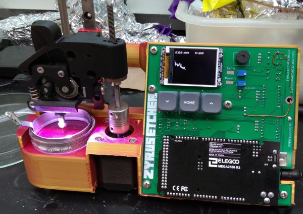
That’s exactly what [Baird]’s device does: a Petri dish on a 3D printed frame holds a volume of sodium hydroxide solution, while a jackscrew Z-stage moves a probe holder up and down. A piece of tungsten wire is dipped into the solution and a voltage is applied to start the etching process. Because most of the etching happens at the liquid’s surface, the wire gets progressively thinner at that point until it snaps and the bottom half drops off. When this happens, the current through the wire changes rapidly, which triggers the machine to pull the wire out of the solution and stop the etching process.
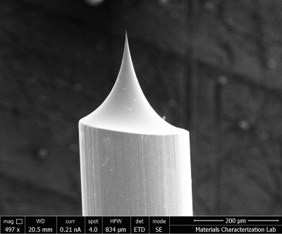
The resulting probes have a well-defined sharp tip with an estimated width of about 50 nanometers — pretty impressive for such a simple setup. The entire hardware design is open source and available on [Baird]’s GitHub page for anyone to replicate. Nanometer-sized needles might only seem useful for those with a professional STM setup, but they also come in handy for all kinds of homebrew atomic-scale imaging experiments.
Continue reading “Homebrew Probe Tip Etcher Makes Amazingly Sharp Needles”


