Building A 3D Printed Scanning Tunneling Microscope

YouTuber [MechnicalRedPanda] has recreated a DIY STM hack we covered about ten years ago, updating it to be primarily 3D-printed, using modern electronics, making it much more accessible to many folks. This simple STM setup utilises a piezoelectric actuator constructed by deliberately cutting a piezo speaker into four quadrants. With individual drive wires attached to the four quadrants. [MechPanda] (re)discovered that piezoelectric ceramic materials are not big fans of soldering heat. Still, in the absence of ultrasonic welding equipment, he did manage to get some wires to take to the surface using low-temperature solder paste.

As you can tell, you can only image conductive samples

A makeshift probe holder was glued on the rear side of the speaker actuator, which was intended to take a super sharp needle-like piece of tungsten wire. Putting the wire in tension and cutting at a sharp angle makes it possible with many attempts to get some usable points. Usable, in this instance, means sharp down the atomic level. The sample platform, actuator mount and all the connecting parts are 3D-printed with PA-CF. This is necessary to achieve enough mechanical stability with normal room temperature fluctuations. Three precision screws are used to level the two platforms in a typical kinematic mount structure, which looks like the only hard-to-source component. A geared stepper motor attached to the probe platform is set up to allow the probe to be carefully advanced towards the sample surface. Continue reading “Building A 3D Printed Scanning Tunneling Microscope”

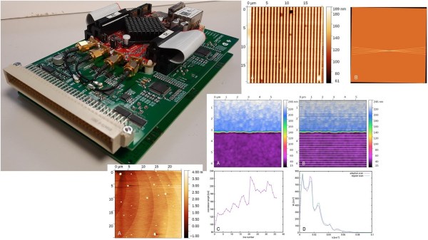
Overview of the Gwyscope SPM controller.

Low-Cost DSP For Scanning Probe Microscopy

A scanning probe microscope comes in a wide variety of flavors, they all produce a set of data points containing the measurements at each location. Usually these data points form a regular 2D grid, but it can be more beneficial to change the density of measurements at certain locations, or even the height, which creates a much more complex probing path and subsequent (XYZ) data set.

Yet this should not deter anyone, as [Miroslav Valtr] and colleagues demonstrate in a July 2023 article in Hardware X where they use a Red Pitaya SBC along with custom Eurocard-format PCBs to create a low-cost-ish (<1,500 USD) open hardware Digital Signal Processor (DSP) they call Gwyscope.

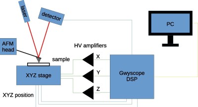
How the Gwyscope controller fits into an example of a scanning probe microscope setup. (Credit: Miroslav Valtr et al., 2023)

The Red Pitaya itself is used as a convenient hybrid FPGA-based module with on-board signal processing hardware, with its Xilinx Zynq ARM-FPGA chip providing both an FPGA section to implement the feedback loop module in Verilog, as well as the means to run a Linux instance with the C-based software that connects via Ethernet to a remote workstation. This communication is based around the GwyFile library, which is part of the Gwyddion project. The scanning paths are generated using libgwyscan (see this presentation for an introduction).

The resulting scan data is saved as an XYZ data file, which can be read with the Gwyddion visualization and analysis program. Although far from a quick & easy afternoon project for the casual hobbyist, it could be a boon for universities and laboratories.

Thanks to [Nicolae Irimia] for the tip.

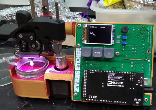
A homebrew machine that dips a piece of wire into an etching solution

Homebrew Probe Tip Etcher Makes Amazingly Sharp Needles

There’s a simple reason why high-tech gadgets like PCs, TVs and smartphones are so cheap: they’re mass-produced. By spreading out huge engineering costs over equally huge production volumes, the cost per item can remain quite low. The flipside to this is that devices with only a small niche market can be extremely expensive even when they seem quite simple.

[Baird Bankovic], an undergrad student at Penn State University, discovered this when he was working with a scanning tunneling microscope (STM). He noticed that the machines used to make STM probes, a pretty straightforward process, cost north of $7500. This inspired him to make a cheap STM probe etching machine using simple homebrew parts.

If you’re not familiar with scanning tunneling microscopy, here’s how it works in a nutshell: a very sharp tungsten needle is positioned a few nanometers above the sample to be analyzed, and a small voltage is applied between the two. Through an effect known as quantum tunneling, a small current then flows between the probe and the sample. By observing this current and scanning the probe across the sample, a three-dimensional picture of the surface is obtained with sub-nanometer-level resolution.

One of the many factors that determine the quality of the image is the sharpness of the probe. Because a very sharp probe is extremely fragile and prone to oxidation, they are typically made on-site by dipping a piece of tungsten wire into an etchant in one of those costly machines.

That’s exactly what [Baird]’s device does: a Petri dish on a 3D printed frame holds a volume of sodium hydroxide solution, while a jackscrew Z-stage moves a probe holder up and down. A piece of tungsten wire is dipped into the solution and a voltage is applied to start the etching process. Because most of the etching happens at the liquid’s surface, the wire gets progressively thinner at that point until it snaps and the bottom half drops off. When this happens, the current through the wire changes rapidly, which triggers the machine to pull the wire out of the solution and stop the etching process.

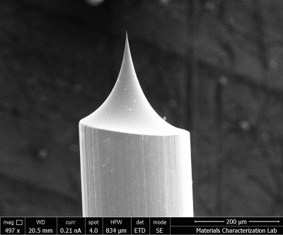
The resulting probes have a well-defined sharp tip with an estimated width of about 50 nanometers — pretty impressive for such a simple setup. The entire hardware design is open source and available on [Baird]’s GitHub page for anyone to replicate. Nanometer-sized needles might only seem useful for those with a professional STM setup, but they also come in handy for all kinds of homebrew atomic-scale imaging experiments.

Continue reading “Homebrew Probe Tip Etcher Makes Amazingly Sharp Needles”

Characterizing Singular Atoms Using X-Ray Spectroscopy And Scanning Tunneling Microscopy

Scanning Tunneling Microscopes (STMs) are amazing tools which can manipulate singular atoms, but they cannot characterize these atoms as they act only on the outer electron shell. Meanwhile X-ray spectroscopy is a great tool for characterizing materials, but has so far been unable to scale down to singular atoms. This is where a recent study (paywalled, see summary article) by Tolulope M. Ajayi and colleagues demonstrates how both STM and X-rays can be combined in order to characterize singular atoms.

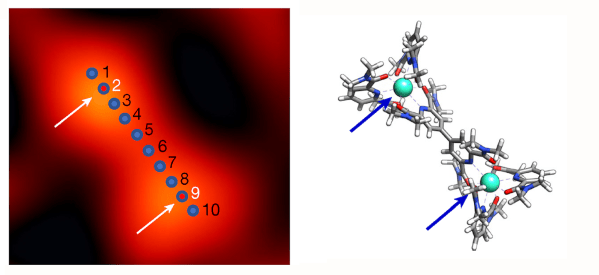
Structure of a part of the supramolecular complex used to measure the x-ray absorption spectrum of a single iron atom. The iron atom (red) is held within several ring-shaped structures. (Credit: Ajayi et al., 2023)

This research builds on previous research on synchrotron X-ray STM (SX-STM) which has been used for nanoscale imaging since 2009, but not down to the scale of a singular atom yet. Key to this achievement was to synthesize supramolecular complexes that could act as ‘tweezers’ to hold the atom under investigation in place and away from atoms of the same species. This not only allowed the atom to be identified using SX-STM, it also demonstrated that more subtle chemical properties of the atom can be analyzed in this manner, such as the way it interacts with other atoms.

The information gleaned this way matches up with what we know about the two atoms used in the study: iron and the rare earth terbium, with the latter’s lack of hybridization of its f orbitals (ℓ = 3) observable. For less well-studied atoms this method could provide a very efficient way to get a detailed overview of its properties. What is more, in future studies the researchers hope to use polarized X-rays to also obtain information about an atom’s spin state, opening interesting possibilities in areas such as spintronics and memory technologies.

Heading image: As the tip was scanned across ten positions in a sample containing two terbium atoms, it picked a signal only from the positions (2 and 9) where terbium was located (left: STM image; right: sketch of the corresponding molecular structure). (Credit: Ajayi et al, 2023)

Scanning Tunneling Microscope Packs The Bits

We don’t usually think of a microscope as an active instrument, but researchers in Canada have used a scanning tunneling microscope to remove or replace single hydrogen atoms from the surface of a hydrogen-passivated silicon wafer. If the scientific paper is too much to wade through, there’s an IEEE Spectrum article and a video that might run on the 6 o’clock news below.

As usual with these research projects, there is good news and there is bad news. The good news is that — in theory — a memory device made using hydrogen lithography could store 138 terabytes per square inch. That’s enough, apparently, to store the entire iTunes catalog on a quarter. The bad news? Well, right now this takes exotic lab equipment at very low temperatures and pressures.

Continue reading “Scanning Tunneling Microscope Packs The Bits”

Hacklet 103 – Piezo Projects

The piezoelectric effect is simple in its rules: Apply mechanical stress to a material and you generate an electric charge. The inverse is also true: Apply a voltage to a material, and it changes shape. This doesn’t work for everything, though. Only certain materials like crystals, some ceramics, and bone have piezoelectric properties. The piezoelectric effect is used quite a bit in electronics, so it’s no surprise that plenty of hacker projects explore this physical phenomena. This week’s Hacklet is all about some of the best projects utilizing the piezoelectric effect on Hackaday.io!
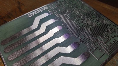
strumWe start with [miro2424] and StrumPad. Strumpad lets you play a MIDI instrument by strumming, just like a guitar. A music keyboard acts as the guitar fretboard here – keys can be pressed to choose notes, but no sound is generated. When the strumpad is strummed, six copper strips act as capacitive sensors. Touching the strips determines which notes will be played. A piezo disc hiding below the circuit board detects how hard the notes have been strummed or tapped. The ATmega328 running the strumpad then passes the velocity and note-on MIDI messages on to a synth.
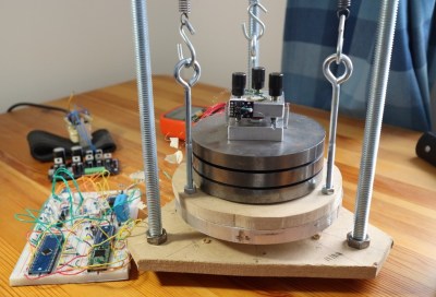
stmNext up is [Dan Berard] with Scanning Tunneling Microscope. Inspired by a project from [John Alexander], [Dan] created his own Scanning Tunneling Microscope (STM). The key to an instrument like this is precise movement. [Dan] achieves that by using a normal piezo disk. These disks are used as speakers and buzzers in everything from smoke detectors to greeting cards, so they’re common and cheap. [Dan] cut his piezo disk electrode into quadrants. Carefully controlling the voltage applied to the quadrants allows [Dan] to move his STM tip in X, Y, and Z. Incredibly, this microscope is able to create images at the atomic scale.
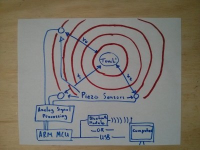
touchboard[Thatcher Chamberlin] is next with Low-Cost Touchscreen Anywhere. [Thatcher] used a trio of Piezo disks to make any flat surface touch sensitive. The three sensors are placed at 3 corners of a rectangle. Touches with the rectangle will create vibrations in the surface that are transmitted to the piezo sensors. By measuring the vibration time of arrival, it should be possible to determine where the surface was touched. This kind of measurement requires a decent processor, so [Thatcher] is using the ARM Cortex-M0 in NXP’s LPC1114FN28. Initial tests were promising, but we haven’t heard much from [Thatcher] on this project. If you see him online, tell him to hurry up! We’re hoping to turn our parking lot into a giant electronic chess board!
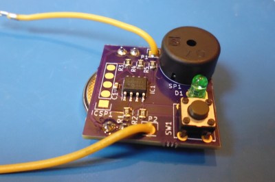
contFinally, we have [Jose Ignacio Romero] with Low Power Continuity Tester. [Jose] used a Piezo element in a slightly more mundane way – as a buzzer. Who needs a whole multimeter when you’re just trying to check continuity on a few circuits? This continuity tester uses a PIC12LF1571 processor to find open and short circuits. The 5 10 bit ADC in the PIC is plenty of resolution for this sort of tester. In fact, [Jose] even included a diode test, which emits a short beep if the leads are placed across a working diode. The PIC processor uses so little power that this tester should run for around 800 hours on a CR2032 watch battery.


If you want to see more piezo projects check out our brand new piezo projects list! If I missed your project, don’t get buzzed! Drop me a message on Hackaday.io, and I’ll add it to the list. That’s it for this week’s Hacklet. As always, see you next week. Same hack time, same hack channel, bringing you the best of Hackaday.io!
Quantum Mechanics In Your Processor: Tunneling And Transistors

By the turn of the 19th century, most scientists were convinced that the natural world was composed of atoms. [Einstein’s] 1905 paper on Brownian motion, which links the behavior of tiny particles suspended in a liquid to the movement of atoms put the nail in the coffin of the anti-atom crowd. No one could actually see atoms, however. The typical size of a single atom ranges from 30 to 300 picometers. With the wavelength of visible light coming in at a whopping 400 – 700 nanometers, it is simply not possible to “see” an atom. Not possible with visible light, that is. It was the summer of 1982 when Gerd Binnig and Heinrich Rohrer, two researchers at IBM’s Zurich Research Laboratory, show to the world the first ever visual image of an atomic structure. They would be awarded the Nobel prize in physics for their invention in 1986.

The Scanning Tunneling Microscope

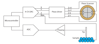
IBM’s Scanning Tunneling Microscope, or STM for short, uses an atomically sharp needle that passes over the surface of an (electrically conductive) object – the distance between the tip and object being just a few hundred picometers, or the diameter of a large atom.

stm
[Image Source]
A small voltage is applied between the needle and the object. Electrons ‘move’ from the object to the needle tip. The needle scans the object, much like a CRT screen is scanned. A current from the object to the needed is measured. The tip of the needle is moved up and down so that this current value does not change, thus allowing the needle to perfectly contour the object as it scans. If one makes a visual image of the current values after the scan is complete, individual atoms become recognizable. Some of this might sound familiar, as we’ve seen a handful of people make electron microscopes from scratch. What we’re going to focus on in this article is how these electrons ‘move’ from the object to the needle. Unless you’re well versed in quantum mechanics, the answer might just leave your jaw in the same position as this image will from a home built STM machine.

Continue reading “Quantum Mechanics In Your Processor: Tunneling And Transistors”