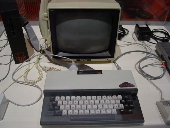
[Brad Robinson] was feeling a bit nostalgic for his Microbee, so he rebuilt it in an FPGA. Not once, but three times. For the uninitiated, the Applied Technology Microbee was a Z80 based computer 1980’s. Designed in Australia, the Microbee did not see much popularity outside its home continent. Even so, the introduction to home computers many Australians was on a Microbee. [Brad] actually wrote several programs for the Microbee, including some games sold by Applied Technology themselves.
Fast forward to 2012, [Brad] is learning FPGAs, and wants to build a Microbee in VHDL. The FPGAbee was born. The first iteration of the FPGAbee began with the CPU, which came from the T80 open source VHDL Z80 core. Around this core [Brad] added the video controller, keyboard, and sound. When he started adding disk functionality, [Brad] ran into some problems. He wanted to use a FAT formatted SD card for cassette and hard disk emulation.
The relative complexities of the FAT format meant he would have to use some custom software to make this work. [Brad] decided to run this software on a second Z80 core. Both cores would need access to memory, and this is where [Brad] learned what he calls “a hard lesson in cross domain clocks” on FPGAs. Multiple clock nets can cause major propagation delay issues. [Brad] was able to work through the problems, but it caused him to step back and re-evaluate the entire design. This was the start of FPGABee2.
Continue reading “Build An FPGA Microbee In Three (Not So) Easy Steps”