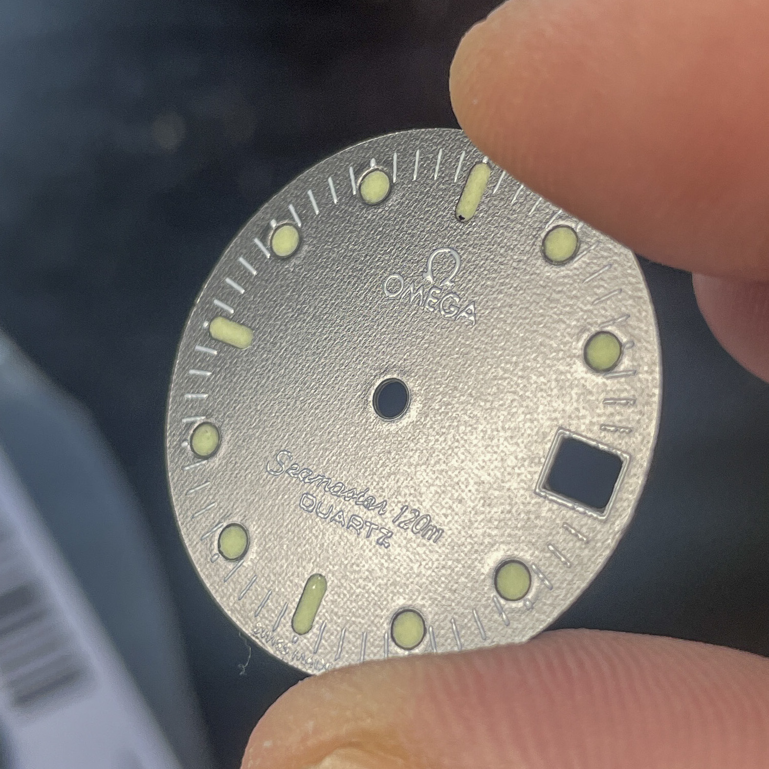
[STR-Alorman] is into vintage watches, particularly Omega Seamaster quartz numbers from the 1980s. Among his favorites is the Seamaster Calypso III, a precious few of which were created in a lovely and rare black-on-black colorway. [STR-Alorman] found one on online, but it had a number of problems including a scratched-up face. Having done a respectable amount of PCB design and assembly, he decided to make a new face and have it fabbed.
The one angle where you can even tell this is a PCB.
After taking scale-referenced photos with a DSLR, [STR-Alorman] created vectors in Illustrator and then ported those to KiCad. He sent two versions to the board house — one with holes at index points, and one without — because he wasn’t sure which would be better for applying the luminization compound that makes them glow. Spoiler alert: it was the one with the cutouts.
Once this was done, [STR-Alorman] reassembled the movement, which doesn’t look easy at all, and involved getting the height of a bit of CA glue just right so as not to interfere with the movement of the date wheel. He replaced the bezel insert, re-luminized the hands, and now has a beautiful timepiece.
We believe only the nerdiest of nerds could tell this is a PCB, and they would need exactly the right light to make that determination. Here’s a watch that leaves no doubt about it.
The semiconductor devices were put to the test under different atmospheres in this chamber.
One of the humbling things about writing for Hackaday comes when we encounter our readership and learn the breadth of our community and the huge variety of skills and professions you represent. Among your number are a significant representation among scientists, and as a result we often receive fascinating previews of and insights into their work. Sometimes they deserve a little bit more attention than one of our normal short daily pieces, and such a moment has come our way this week.
We’ve been fortunate enough to have an early look at a paper which makes detailed observations of a hitherto barely characterised property of semiconductor junctions that might have some interest for Hackaday readers in their work. In their paper, [Mellie], [Bacon] et al at Fulchester University in northeast England take a look at incandescent luminescence, a fleeting and curious effect exhibited by all semiconductor junctions in which they emit short-duration high-intensity infra-red and visible light with an extremely fast rise time when presented with high levels of current. This is a property which has been rarely exploited in commercial devices due to the large current densities required to reproduce it.
Incandescent Luminescence Explained
If you’ve never heard of incandescent luminescence before then you’re in good company, for neither had we until it was explained to us. It appears that there are a set of higher energy state conductivity bands in a semiconductor junction that can only be reached once the current passing through it breaches a threshold governed by the available quantum plasma dipole moment of the semiconductor material in question. At this point the junction assumes a plasma condition resulting in the abrupt emission of infra-red and visible radiation, the incandescent luminescence phase has been triggered.
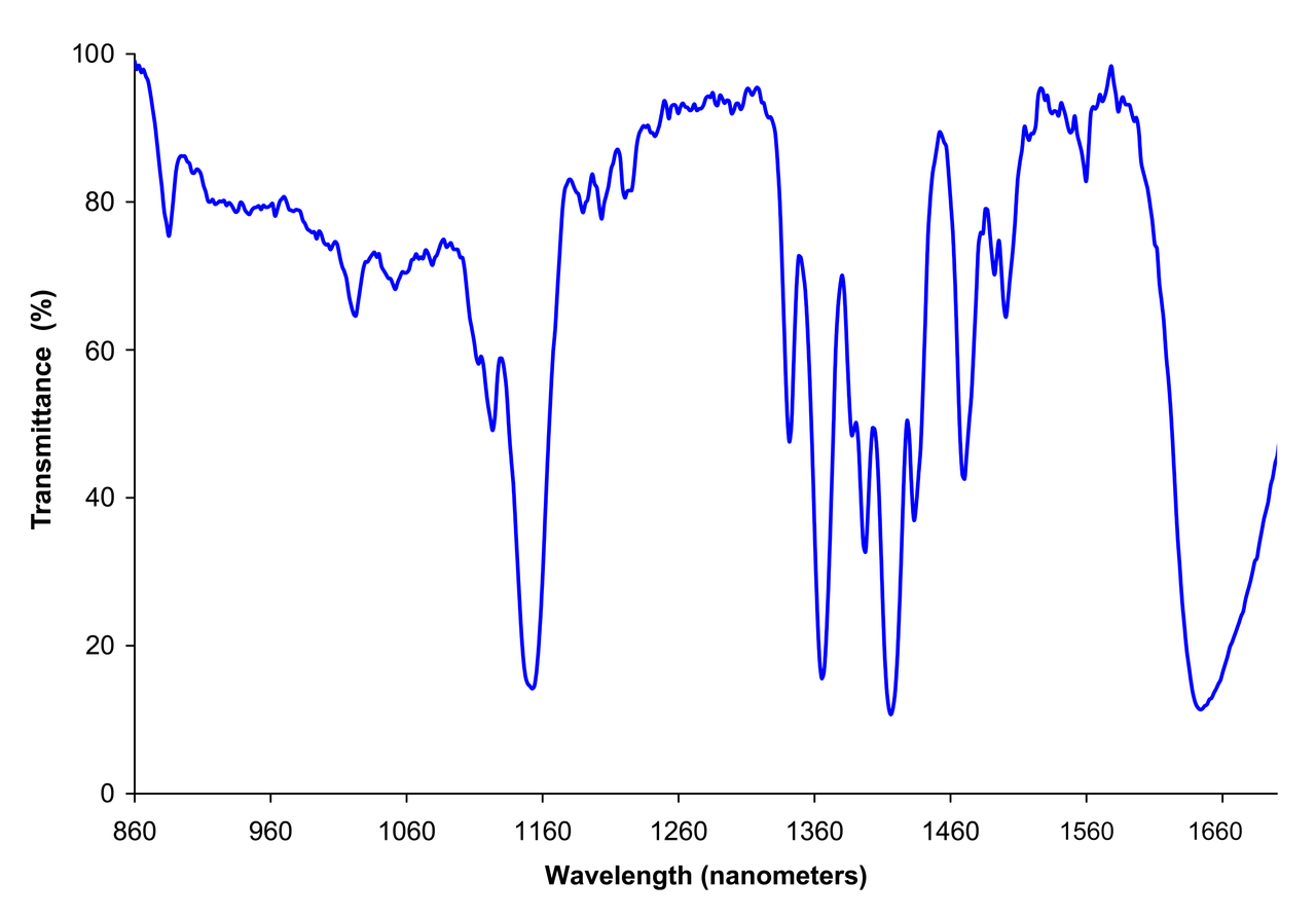
A near-infra-red spectrum of incandescent luminescence in a silicon semiconductor junction.
Though it has been known to science since first being observed in the early 20th century by the earliest experimenters in the field of semiconductor junctions, the transitory nature of the phenomenon has traditionally been a barrier to its proper examination. The British team took a selection of commercial semiconductor devices very similar to the types that might be used by Hackaday readers, placed them in a chamber, and used an array of photoelectric sensors coupled with ionising detectors using americium-241 alpha radiation sources to measure their emissions.
The resulting data was then harvested for processing through a stack of custom high-speed ADC cards. Current densities from as low as a few milliamps to hundreds of amps were tested across forward-biased PN diode junctions using a computer-controlled DC power supply, resulting in a variety of spectra and showing the resulting thermionic photon emission at higher currents to have a preponderance in the infra-red region.
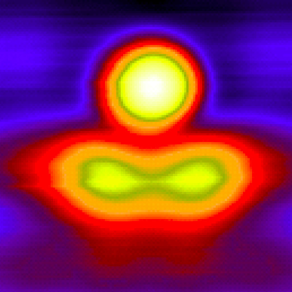
Incandescent luminescence in action, through an infra-red pyrometer.
A series of experiments were conducted to investigate a related effect first described by those early scientists in the field: that the atmosphere in which the semiconductor junction sits has a significant effect on the way it exhibits incandescent luminescence. Bathing it in gaseous CO₂ or nitrogen was found to reduce the phenomenon by as much as 95%, while immersing it in liquid nitrogen resulted in it becoming completely unobservable. Oxygen-rich atmospheres by comparison served to enhance the luminescence observed, to the point that in one of pure oxygen it reached an efficiency level of 100%.
The high conversion efficiencies and rapid onset of incandescent luminescence once it has been triggered compares favourably to those of existing devices such as LEDs or wire-wound resistors used where either infra-red or visible light is required. The researchers expect the effect to be exploited in such product families as photographic flash generators, electronic igniters, and other short-duration high-intensity applications. Given their obvious advantages, we’d expect their effects on those particular markets to be nothing short of incendiary.
Thanks Ellie D. Martin-Eberhardt for some invaluable inspiration and technical help with covering this story.
Sonoluminescence is one of those strange phenomenon that many would never encounter outside an academic environment. For those who have never heard of it, Sonoluminescence is when tiny bubbles suspended in a liquid emit light while being vibrated at certain frequencies. We were pleased to see that some plans are out there on how to build your own device to produce it.