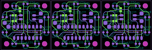
A lot of the board houses out there including Seeed and ITead studios have a fixed size for circuit boards before the price goes up. A one-inch square board costs the same as a much larger 5cm x 5cm board, making panelized PCBs a great way to get more boards for the same amount of money. Trying to panelize a board in Eagle with copy and paste is a chore without the right tools, though, so we’re happy to see a great panelization tutorial from [Victor].
To panelize one of his boards for a PCB order, [Victor] used one of Eagle’s User Language Programs to duplicate the part names on the additional boards. After that, it was a simple matter of running a CAM job to generate the necessary Gerber files.
Of course once the boards arrive, you’ll have to cut them apart from each other. This can be done with everything from a Dremel to a hack saw to a metal shear, but we’re wondering what other Hackaday readers are using to cut up PCBs. Leave a note in the comments with your preferred method of depanelization.


A heavy duty paper cutter can be used to cut circuit boards. There may a problem with excessive bending, though.
I’m experimenting with this teensy little table saw I got from Harbor Freight, with a diamond cutoff blade – http://www.harborfreight.com/4-inch-mighty-mite-table-saw-93211.html Seems to work, although I had to build some legs for it to keep it from tipping over and slicing parts of me off. I had to make my own fence, too.
Any details on your fence or anti-tip mods?
The fence is a little chunk of 1″ aluminum angle, c-clamped to the table. The legs are just two lengths of scrap wood about half again the length of the table, screwed into the holes where the incredibly ineffectual little rubber feet that come with the saw originally went.
Maybe this is an idea? http://www.youtube.com/watch?v=Vlyc2wEsak4
This would work if the manufacturers allowed v grooving the boards on panelized orders, which in this case both Itead and Seeed don’t allow.
You can also use a diamond cutter with a dremel, as long as your hands are somewhat steady it works perfectly fine.
Itead allow vgroove if pcb is at least 7cm in one size.
they don’t write it but they can if ask nicely :D
PROXXON – KS 230 tablesaw + diamond blade.
not the cheapest investment but it pays.
the diamondblade was kind of hard to find locally but it lasts now since a couple of months.
it is 0.5mm in width and in your panelized designs you should leave 0.6mm space between the boards.
that works like a charm.
also important: when you do a ratsnest and have copperfilled areas make sure that they are at least 0.5mm away from the absolut border.
else you get ugly copperripples.
i see designs without ratsnest all the time (like the one in this post) but i can highly recommend doing that.
you draw a polygone around your board on the top layer and bottom layer then use the name command and call those polygones GND.
now you do not have to connect all the ground pins by hand as they are connected to the ratsnet.
of course you can make one layer VCC and the other one GND but i was told that this is not “how its done” :)
That is how it is done, maybe not for so much 2 layers, but for 4 layers is is normal to use the two inner layers almost exclusively for supply and gnd and the outer layers for signals. In the old days (think paper and black tape) those supply and gnd planes were normally drawn in reverse and then inverted
My last 5cm x 5cm boards I received from Seeed earlier this month were V-grooved. They just snapped cleanly. Only had 2 boards per panel though.
How did you add the vgrooves into the eagle file?
I use DipTrace, but I didn’t even add them. They just did it automatically in between the board outline of the two panels. Here’s a gerber render of the entire panel: http://www.flickr.com/photos/sporadic/8498123883/in/photostream
V-score or tab routing
I use a small tile saw with diamond blade [for cutting ceramic tiles] – goes thru PCB’s like a hot knife thru butter – I just leave 1/16″ gap between boards, and put a 1/8″ hole at inside corners.
I also use a sheet metal nibbling tool for inside corners.
I’ve used a tile saw before with a diamond blade. Works pretty well and actually filling up the water tray keeps a lot of the fibreglass dust out of the air!
Now I have a CNC machine I just use that. There’s plenty of cheap sources for routing bits that eat through fibreglass like butter.
would a bandsaw work?
I’ve used a band saw to cut PCBs before, just make sure the band saw has a fairly high tooth count, can’t remember what blade I was using but too low and a lot of things can go wrong (break the blade, shatter the board, etc)
Could we pick one unit of measure and stick with it, at least in the same sentence?
Heavy duty paper cutters work great for separating bunches of boards.
I use a $30 tile saw I got off craigslist. It has a 7″ diamond blade. As others have said, it cuts really clean. I leave 3mm between panels. I like cutting the boards wet, it really limits the dust but is abit of a mess. .I put a piece of plexi on the saw table and cut free-hand w/o fence.
Found the biggest pair of tin snips Home Despot had. They worked pretty well for the small (1″ by 1/2″) boards I needed to split up.
Better yet: I had the next batch made at BatchPCB, and they split them for me!
Best 165.00 I spent in my DIY circuit boards. I know its an investment but I never struggle cutting a single board again. Its a shop fox M1041 Plate Sheer 12 Inch and cuts PCB;s of any size perfectly everytime. Don’t recall where I saw the video that introduced me to it but I was sold when I saw it and glad I made the plunge.
http://www.amazon.com/gp/product/B0039ZAASK/ref=oh_details_o03_s00_i00?ie=UTF8&psc=1
A really simple way that works surprisingly well is to make a v-score with a straight edge and razor blade, after a light first pass the score is started and after a few heavier passes you can snap them like a normal vscore. You can get an excellent edge with no fr4 dust being kicked up everywhere or needing to be sucked up with a vacuum, and its really not all that bad when you only a have a few scores to make.
Can HaD please knock it off with all the Eagle posts, and focus on KiCad instead? Hacking is all about openness and sharing, which closed soured software is most definitely not. Openhardware needs to remain in the spirit of openess and opensource, especially in our tools. Closed source needs to be shunned at every point.
Seriously? Eagle is very popular with DIY, so much that SparkFun has gobs of tutorials and shares Eagle files for nearly every board they sell (in the spirit of Open Hardware, I might add. I have nothing against and in fact support open hardware and software, but really hate when I see posts like this. Take your closed-minded religion elsewhere, please.
I was about to reply, and you said exactly what’s on my mind. Talk about closed-source, how about a closed-source attitude like this gentleman’s.
There was a discussion on MakeBlog (I think around the time Makerbot did their new closed-source 3D printer) about just how far back the design chain you have to go to consider it open-source. It is surely enough to make the files available, so long as they are in SOME format that’s readable, without actually being forced to design the whole thing in a particular open-source package. E.g. SparkFun or Dangerous Prototypes with their Eagle libraries – you can easily share the Eagle files, and others will be able to open them. Or you could share the Gerber files, which is what board houses want anyway.
To be honest, I think that even a schematic and image of the board layout would be enough – then, anyone can redraw it in whatever application they choose.
Eagle has such an established user base, a vast library of components and scripts/programs, that it isn’t going to disappear any time soon!
Right as rain the software used does not dictate the openness of the design. It’s like code written for Visual Studio; not any less open source. As far as I’m concerned open hardware only requires a schematic – in any format…. gerbers would be nice, but not required.
I agree that eagle has a strangle hold on this market and it’s awful software to boot, but that doesn’t make any design in it invalid or any less open.
How do you feel about the posts that use matlab or autocad or labview; all very expensive and closed source with lots of FOSS alternatives (not necessarily viable FOSS alternatives) but it doesn’t detract from the validity of the HAD post or of the hack.
That isn’t saying much. Sparkfun is in the wrong too, the files they post need to be in an Open format like KiCad files and libraries instead of Eagle.
You cannot dictate to a commercial entity what they need to do. You are free to start our own store and publish whatever files you want. I might even buy something from you. But you aren’t going to do that are you – that’s what I thought.
Eagle is one of the most widely used programs by the electronics hobby community. For me, it can turn my designs into g-code for a CNC router to cut my own PCBs. The freeware version has not limited me so far. Kicad is also good however I can’t cut my own PCBs with it (yet).
Why not? I can tell you why not:
http://daid.mine.nu/blag/2011/11/10/kicad-alternative-for-eagle/
I’m glad to see some of the problems listed. Talk about clunky. I bet it has problems (if it’s even possible) of doing gate swap, pin swap, part replace, all of which I use regularly in Eagle. Why on earth converting to a PCB should be so difficult. That’s a good thing with Eagle – parts are very tightly tied to their packages, so converting between schematic and PCB is very easy.
And it doesn’t automatically place part names and values?!? Jeez….
There would also appear to be a lack of an Eagle-style command prompt in KiCad. This is very powerful in Eagle – things like “mov (C> 0 0) (R -0.5 -0.5)” which moves the group selected by clicking at (0,0) by a relative distance of (-0.5,-0.5), stuff like that. It’s even quicker than clicking buttons with the mouse – if I want to change track widths, I just type “ch wi 20” which CHanges the WIdth to 20 units, and then start clicking.
Hehe, i’m using an ordinary scissors to cut my PCBs. Of course the PCB must be tops 1mm or it wont work. :)
But another way to panelize, whick i prefer, is to just open gerbv and modify the gerbers by copying the PCB, layer by layer. That way you can also see in real time does your PCB exceed the limits.
I use several PCB layout software packages, one of my least favourite ones is Eagle, but when traveling I am forced to use it as Cadence is a little big for a laptop.
To panelise in Eagle, with the board layout open, I save it into a temporary directory, which also copies the schematic along with it.
Close Eagle, the delete the .SCH from the temporary directory.
Re-open the .BRD file in Eagle and simply copy and paste the board to the required number. No back-chat from Eagle about component numbers and changing the schematic!
I have excellent relations with my PCG house, so I make an excessive number of panels and they simply delete them to their requirements.
Before you panelize, look at $/sqcm. I made a little table of Seeed prices and it is horribly inconsistent. Not all sizes have the same economy of scale you’d expect. There is obviously competitive pressure on the 5×5 and 10x10cm boards – good!