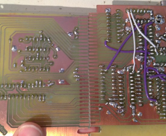
While this is not exactly a hack or a fail, it definitely is an inspiring example on how to debug a faulty card.
[Quinn] is one of the very few hobbyists out there that designed her own 6502 based computer. For the young readers of Hackaday, the MOS 6502 was introduced in 1975 and has been used in the Aple // line, the Commodore 64, the Vic-20, the Atari computers, the Nintendo Enterntainment System and others.
[Quinn]’s homemade new RAM board had been working for many weeks until it started to show some weaknesses by only sporadically passing the boot RAM test. Assuming the RAM was the problem, she started by making a more advanced memory test, which showed errors at random addresses.
She didn’t have any more of the same memory chips on hand which could be used with a fresh PCB. Determined to power through the issue, she etched a new board with a new memory design. Unfortunately it also gave memory errors at boot. Only one culprit was left, which is shown in the picture above. It’s a small sizing error in the board artwork which was just enough to cause a misalignment on the connector.
The article contains many details about her debugging process, so it definitely is worth the read.


Good read.
Haven’t seen stacked RAM chips since modifying an Atari 800 RAM board to add 256KB, accessible as a RAMdisk. Was the second electronics project I ever did. Nostalgic!
Commodore got a LOT of mileage out the 6502. It was also in their PET and CBM products.
I’ve made that mistake before, damn page scaling when printing before I do the iron-toner-transfer method.
Drill out all the holes, Solder SMD’s fine, resistors look to be a bit tight, but when you put the last big 2×20 male header in… NOPE! off by an effing hair (or 10)
Me too
Add me to the page scaling list lol. I loved reading the write up on this as it is one of those heart-breaking things that happens. It is always nice to find a solution and especially in Quinns case as the chips were hard to get so ya really pray it isn’t that. I reckon everything was slid in just right the first couple of times and things expanded with heat as they were used causing that micrometer gap to bridge. One of those things like “always backup your data” and “always check your optics” that is a painful lesson at any age. Kudos to Quinn! Keep hammering away! We love reading about your adventures with Veronica and I learn something everytime :)
Always print on regular paper first when using toner transfer method, and use you micrometer to check dimensions before printing the actual transfer print….
I built a 4K(!) RAM expansion card for my Ohio Scientific back in those days, using 2114’s I recall. When I plugged in the (wirewrapped) board, the computer’s power supply sagged below 5V. I then substituted a bigger supply, thinking the original one was inadequate. The computer booted OK on the larger supply but failed to “see” the extra memory. When I smelled something starting to get warm, I ran my index finger across the backs of the RAM chips. My finger got stuck to the one that was mounted backwards. It only took 2 months to regrow my fingerprint.
This should be in HAD Fail.
First assembly, hold at entrance and see ‘did I get it right’
Just touch each one quickly, like a skillet.
I parted out a full sized microwave sized dual 8′ floppy disc from Ohio Scientific. I saved the boards and motors.
Honestly, this is why making boards at home are not worth it. Send the eagle files to Sparkfun and have them make professional boards for you.
She must have been almost asleep to miss that when she plugged it in the edge connector. Working far too late into the night will really cause brain cramps.
This is exactly the kind of board that is worth making at home. Large pitch, large board, few holes, single sided, mostly empty, one-off – and stupidly expensive to have made for you. Assuming it’s 4″ x 6″, that would cost $120 at OSH Park. For a board that supports maybe $3 of components?
If I were making a similar computer and wanted to avoid home-etched boards, I might consider having a pro PCB service make me a panel full of nothing but edge connectors, that could be attached to perfboard, then wired up elm-chan style. Nothing more.
True, but it is also possible that the board’s simplicity is partly the result of the requirement that it can be made at home.
On a professionally made board, you can put the whole computer on a single PCB.
I’d call that a huge sizing error rather than a small one
It was small enough to work some of the time. That’s way worse than being off enough that connections were never being made (which you can trouble shoot with a continuity test).
On a recent PCB design I put small bumps along two adjacent, straight outside edges of the copper pour. The bumps were spaced 10mm apart so that if anyone had to scale it before printing, it would be very easy to confirm that the scaling was right with a ruler, and if not, estimate how much to adjust it by. YMMV.