Oh that title is so misleading. But if you squint your eyes and scratch your noggin it’s almost true. Thanks to the hard work of [Peter Lawrence] it is now possible to hack together an extremely inexpensive CMSIS-DAP ARM debugger.
Let’s talk about function and we’ll get back to cost later. CMSIS-DAP is a standard that gives you the kind of breakpoint control you expect from a proper debugger. In this case [Peter] implemented the standard using 4k words of space on a PIC 16F1454. This lets it talk to the debug port on ARM chips, and the bootloader (also written by him) doubles as a USB-to-UART bridge. Boom, done. OpenOCD (and a couple of other software packages) talks to the PIC and it talks to the ARM. Nice.
Back to the cost question. You can get a 16F1454 for nearly a dollar when you order in quantity. If you cut up an old USB cable, recycle some jumper wire, and already have power and decoupling on hand, you’re in business for nearly one dollar.


flippin sweet
Really cool, I can understand his pain as I also dug into the specifics for SWD a little.
Just one question: Where is the code? Come on, why do you post hacks without the code?
Get a local copy of the pic16f1454-bootloader repository with this command:
hg clone https://code.google.com/p/pic16f1454-bootloader/
Yes, but that is just the bootloader. I can not find the code for the debugger itself, which is the topic of the article.
I hadn’t noticed this when writing the feature. I just shot of an email to Peter asking if he’s planning to make it available. I’ll update when I hear back.
I posted a detailed reply further below; my hands are tied by the ARM EULA.
I love the 5.25″ floppy disk form factor!
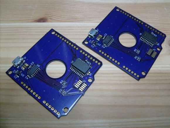
Except shrunk to half the size… It’s Arduino form factor with a hole in the middle
Why is it designed that way? I read the entire page but I didn’t see the answer.
I was trying to think of cheap ways to ship the PCB; the hole allows it to fit in a CD/DVD case. So, recycle existing CD cases and use existing media mailers.
Groovy, but ST is pushing STM32F0 parts for $0.32 in quantity, so PIC seems on the pricey side. Imagine that. More importantly, it would be a fun feature to program and debug the debugger with another one of the same debuggers. :)
That’s what STM does with the Discovery Boards, right? There are two F series ARM chips on there, one is the ST-Link, the other the target.
If we can get our hands on the code from Peter I’m sure it would be trivial to port it to ARM. Can you make a truly sub-$1 ARM debugger? (don’t forget to write about it and send us a link!)
If you want code for ARM, go here:
http://mbed.org/handbook/cmsis-dap-interface-firmware
This is a bit more than just debugger as it has Mass Storage for drag & drop for downloading, serial port etc.
Their source code is in the github URL listed in first paragraph. They
even tell you what’s needed to port it to a new chip.
Right now I’m busy on another project, but I would like to have a small debugger that fits into a USB cable and attaches to the 1.27mm by 6 pin SWD interface that’s commonly used in discovery kits as well as some other STM32 kits. The STM32F0 in 4x4mm 28 pin package would be ideal for this purpose. I will not be able to get to it until at least April, though.
STM32F0 doesn’t have a USB SIE. Unless/until there is a software bit banging USB implementation, that comparison is moot. The closest ARM with USB support is around $1 range Freescale KL2x family.
There are several F0 models that have USB. The most interesting ones are brand new, but there have been F0 parts with USB “in the wild” for a bit. (http://www.st.com/st-web-ui/static/active/en/resource/technical/document/data_brief/DM00099204.pdf)
What’s more, they have 48 MHz ring oscillators that are accurate enough to do USB without an external crystal. In distribution, the cost is about $1. Buying direct will be quite a bit less if you can swing it.
Thanks for the pointer on the STM32F042xx! I was not aware of this part, but it looks very promising. I haven’t found a distributor that stocks it yet, but will keep looking.
>What’s more, they have 48 MHz ring oscillators that are accurate enough to do USB without an external crystal. In distribution, the cost is about $1. Buying direct will be quite a bit less if you can swing it.
Actually the have an adjustable oscillator that syncs to the USB keepalive pulses in their USB phys. The 48MHz main is probably not more accurate than other RC-oscillator.
Right now outisde of samples, it might as well be made with unobtainium. Findchips returns nothing. Just have to wait a while for it.
I like their TSSOP package as I can also route tracks between 2 rows of pins. 0.65mm pitch is workable.
Jiik, the ugliest PCB layout i’ve ever seen…
It looks like it was automatically routed using TopoR:
http://www.toporouter.com/index.php
Congrats, Nsn! You are the only one who got it correct.
its god awful
Very much agreed :P
haha I was wondering if I was the only one who got his eyes bleeding from watching the picture
Come on guys, that board would be impossible to hand route, are you insane?
It hurt me in the OCD. =(. That said, my first PCB totally looked like that. Then I had to sneak in an extra wire and realized the joys of 45 degree routing.
On a constructive note though, it could use some more groundplane stitching (using vias to connect the top-layer and bottom-layer ground planes together.) It would also be helpful to increase the distance between the traces that run between U1 and U4. Your trace size can probably also be increased slightly. If you go up to 10 mil traces with 10-20 mil separation, then it brings the PCB cost down and increases yield significantly from your board house.
There’s also quite a bit of floating copper. I’m not sure what CAD package was used, but there should be an option in the plane object to remove floating copper. It’s a good idea to remove small bits of floating copper that lies between traces unless you’re a weird RF guy that knows what they’re doing. The floating copper capacitively couples traces together (usually undesired) and also makes it much more difficult to cut and jumper traces during board bringup.
Cool project though. Cheap debug tools are always mega useful (especially if you can get that sort of thing into classrooms.). Also, +1 for the Saleae protocol analyzer.
I’m always torn about how many ground plane stitching vias to use. More drill holes generally equals more cost.
It is a fair criticism; there are design features on this particular board that are not conducive to the lowest build cost. This was based on design rules that have worked fine with OSH Park, so I didn’t worry much. However, I have since done a different form-factor board (not yet arrived) where I deliberately tried to tweak things for maximum yield from cheap houses.
I use DipTrace for my hobbyist boards, and I’ve not aware of a good way of removing floating copper with that software.
To remove unconnected islands in DipTrace, open the copper pour properties window. On the “Pouring” tab, check the “Unconnected” checkbox under “Island Removal”. This should remove any copper in your pour that’s left floating.
For digital signals, it is low impedance (tens of ohms). The noise type
you have to worry about is a current source – magnetically coupled.
You want to look at the return path. i.e. if your chip is driving
current out, there is a return current that goes back into the chip to
complete the loop. If the track is above a power/ground plane, the
lowest inductance path is directly under that trace on the plane. If
there isn’t one, you have to make sure that the (current) loop area
(i.e. inductance) is small.
If there isn’t a plane, the current would seek whatever lowest
inductance path it can find. If that’s another signal track and you have
crosstalk issues!
Now if all your tracks are on one side of the board (no vias) and the
plane(s) are unbroken, you would only need to punch ground vias only at
the source & destination. If your plane is broken by track(s), you would
need to stitch it to make a return path. If your tracks switches layers,
probably should have ground via so that the return current can follow.
Not the worse layout, but can use some clean up on those tracks to go 45 degrees instead of whatever degrees happens to connect the nets without shorting.
Not a big fan of the routing obviously, I wish more people would route boards themselves instead of resorting to the autorouter. (it’s fun!)
Totally agree! Manual routing is an exciting puzzle, much better than sudoku and crosswords, and more addictive than Angry Birds or Candy Crush, lol!
I hand route my boards as I etch my own board with toner transfer, so vias are a pain. I
try to minimize the use, making them accessible (not under SMT packages) and not to route between layers using through hole connectors etc.
The way I see it is that if you are paying to your boards made, might as well use the auto router in Eagle and let it use as many vias to get the job done.
BTW Eagle uses 45 degrees for routing.
I believe you can use an auto-router anyway by setting the via cost to be very high and/or setting the maximum number of vias to zero, etc. You can also increase the separation parameters enough that any vias will never end up under a component, or manually move them- auto-routing and hand routing aren’t mutually exclusive.
I tend to find the auto-router useful in that it can do a lot of the grunt work, but I will have to tweak and hand route portions of the board no matter what. One strategy I have found is to hand route any critical paths, have the auto-router figure out the rest, and then tweak the end result by hand.
I also find that, in Eagle, using the auto-router is almost necessary because Eagle doesn’t have live DRC checking. If it did, I think I would use the auto-router a lot less.
I dislike using the autorouter since it (at least in Eagle) doesn’t know everything about the traces that you do. Doing the work manually allows you to pick where your noisy traces go, how power will flow through the board, etc, etc, etc.
Granted this board has no real high-speed requirements or high-power issues, so there will likely be little issue with autorouter
Really, for me, manually routing a pcb is an almost therapeutic exercise that I like to do to take my mind off of things. I have about a 10:1 ratio of boards that I’ve routed to boards that I’ve actually fabbed/soldered/used.
the electrons get bummed out when they are asked to travel at strange angle
I wonder if this can remove the tracking features that come in the processor?
Anyone else chuckle after spotting madness.c and reading it?
I have very little experience with the PIC family. Can you explain what this code accomplishes? (I don’t even understand the ROM directive)
Directive to store nonvolatile data into code space. (Harvard architecture)
Similiar to the following for AVR code in GCC.
const __flash uint8_t foo[70];
Clever hack! Do I see an Arduino shield PCB form factor? Any relationships with that insanely popular hacking platform :-) ?
All, I’m in a jam as far as my source code implementing CMSIS-DAP on a PIC is concerned.
To get access to the CMSIS-DAP specification, I had to agree to a EULA. Even though I didn’t use ARM’s source code examples, it has a bunch of legalese of how the specification can be used.
I’d encourage anyone who wants to see CMSIS-DAP source code to check out this code (which ARM apparently released under a more liberal Apache license):
https://github.com/mbedmicro/CMSIS-DAP/tree/master/interface/Common/src
There were far fewer complications with the PIC code, and so I was able to open that up (apart from Microchip’s USB library itself) and post it on Google Code. I’m really hopeful that this can enable some interesting and cheap hacks with the PIC bootloader. Users can load anything that they can dream up; the device isn’t made of unobtainium and it comes in easier to solder packages.
What about distributing binary, at least?
I have PIC16F1454 in DIP package eagerly sitting on my table, waiting to be used as ARM debugger – for another DIP ARM part.
But the specification can be used to develop your own CMSIS-DAP code, and to distribute it, even in source code. Look at clause 1 (i) (b): is explicitly says you can distribute the firmware you developed. The only restriction which is interesting is that the firmware must be used for ARM targets only (but it doesn’t matter on what processor the firmware runs). So when you don’t use the supplied firmware, you should be fine (for that derived code cannot be distributedf, but that could be circumvented by using the mbed firmware with its Apache license)
Yes, but Clause 1(i)(b) says that it is subject to Clause 1(iv). Clause 1(iv) includes stipulation that all customers must comply with Clause 1(iv). There is no way to do that with open source.
I’m enthused by the prospect of this STMF042xx mentioned by jpnorair. The chip has some cost-reducing features that could make it competitive with the PIC16F145x. When distributors start stocking it and if ST can sell it cheaply, then we’d have a mandatory ARM.
But you could place your code under the same license as the CMSIS-DAP specification. This should satisfy this condition (since anyone then using it for debugging non-ARM targets is automatically in violation of _your_ license). I know its then not exactly opensource as in GPL, but it might be enough…
>(a) to ensure that they are licensed for use with targets containing microprocessors manufactured or simulated under licence from ARM;
Not like the SWD is going to work on non-ARM chips. Just have to pass down same restriction to users.
> (c) not to use ARM’s name, logo or trademarks to market -any or all
of the CMSIS-DAP Specificationm Firmware,…
Now I think this is the tough part. A debugger to be used with a trademarked product that should remains nameless.
How about simply asking ARM about the situation? Worst thing that could come off it, is that they confirm your interpretation of the EULA.
Nice work! I’m really excited about open source ARM SWD programmers that aren’t based on the difficult OpenOCD code. I’ve been using the McHck for programming a Nordic NRF51822:
http://goo.gl/5aj8IR
This isn’t a full CMSIS-DAP implementation, but it does have flash and gdb-server support.
I’ve been playing around with porting the McHck swd-adaptor to the cheaper KL24 chips (Cortex M0 — about $1.50 in quantity versus $2.20 or so for the MK20 Cortex M4). I’m having a lot of trouble because, unlike the MK20, the KL20 chips don’t seem to “talk” USB correctly without an external crystal, which about cancels out the difference in price. So, I’d love to see this ST chip working.
You probably should be writing firmware if you think openocd is ‘difficult’. Openocd supports cmsis dap by the way and several off the shelf dongles.
Don’t forget NXP’ LPC11UXXXX range like this for example:
http://goo.gl/7jJBQa
Relatively low cost in quantity (@1000) $1.26
regards
Al
Or for something easier to solder LQFP48 for an extra 10 cents :
http://goo.gl/hLfSu6
regards
Al
You free-angle-routing haters are way off base. 45-degree snapping is an aesthetic that simplifies routing and layout software but wastes space and even has worse emi performance than free-angle designs. Check out the circuit board layout for the original NES controller – no autorouter, just beautiful hand-drawn curved traces. The NES MAX controller has a board that has to fit into non-45-degree handles and a 45-degree-snapped layout simply would not fit. Now that the layout software has finally caught up we can use curved lines again.
Update:
Looks like [Peter Lawrence] has posted a version of his work to STM32F072: https://code.google.com/p/dappermime/
A *big* thank you for Peter for releasing his code. His code is so much more straight forward than mbed’s.
I think he has misunderstand what the term “target” means in the ARM license. IMHO it refers to the ARM device you are trying to debug, not whatever dongle handling CMSIS-DAP protocols to facilitate the link.
Thanks to a change in ARM’s terms (3.5+ years later), I was *FINALLY* able to release the source code (the original Dapper Miser PIC16F1454 and subsequent STM32F042/STM320F72 code, not the stopgap Dapper Mime substitute mentioned above): https://github.com/majbthrd/DapperMiser/
I’ve been using and maintaining this Dapper Miser code for years now on my own projects. I really sweated the details to make Dapper Miser as lithe as possible; the code is so lightweight that it is portable to even rudimentary 8-bit USB microcontrollers like the PIC16F1454.
There is also an improved PIC16F1454 USB bootloader that is pure assembly and uses a mere 512 words.
Enjoy!
Great news, thank you much!