If you’ve been thinking about playing around with FPGAs and/or are interested in CPU design, [Domipheus] has started a blog post series that you should check out. Normally we’d wait until the whole series is done to post about it, but it’s looking so good, that we thought we’d share it with you while it’s still in progress. So far, there are five parts.
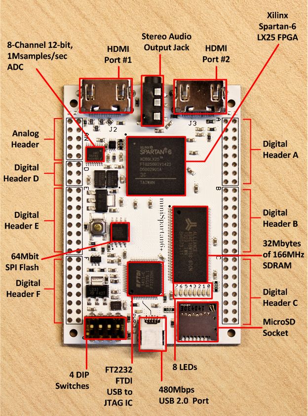 In Part One, [Domipheus] goes through his rationale and plans for the CPU. If you’re at all interested in following along, this post is a must-read. The summary, though, is that he’s aiming to make a stripped-down 16-bit processor on a Spartan 6+ FPGA with basic arithmetic and control flow, and write an assembler for it.
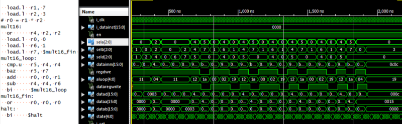
In Part Two, [Domipheus] goes over the nitty-gritty of getting VHDL code rendered and uploaded to the FPGA, and as an example builds up the CPU’s eight registers. If you’re new to FPGAs, pay special attention to the test bench code at the end of the post. Xilinx’s ISE package makes building a test suite for your FPGA code pretty easy, and given the eventual complexity of the system, it’s a great idea to have tests set up for each stage. Testing will be a recurring theme throughout the rest of the posts.
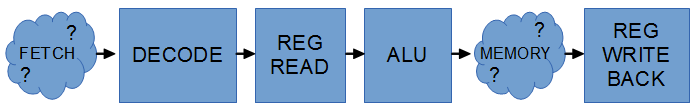
In Part Three, [Domipheus] works through his choices for the instruction set and starts writes up the instruction set decoder. In Part Four, we get to see an ALU and the jump commands are implemented. Part Five builds up a bare-bones control unit and connects the decoder, ALU, and registers together to do some math and count up.
We can’t wait for further installments. If you’re interested in this sort of thing, and are following [Domipheus]’s progress, be sure to let him know: we gotta keep him working.
Of course, this isn’t the first time anyone’s built a soft-CPU in an FPGA. (The OMG was added mostly to go along with the other TLAs.) Here’s a tiny one, a big one, and a bizarre one.


I was mostly interested in that dev board. Grr… missed the kickstarter.
Anyone else know of a board similar to this? One without all the useless crap on it?
dx carries one. http://www.dx.com/p/ep2c5t144-altera-cyclone-ii-fpga-mini-scm-development-board-148979#.Va02UvlVhBc
Having RAM on board is pretty essential, or you’ll waste all your gates making flip-flops for ram.
The one on dx does not have ram, right?
Yeah, RAM was not something I was including as useless crap. I was talking about junk like 7 segment displays, etc..
If the RAM needs are pretty small (kB range) then you can implement them using lookup tables. There are also dedicated block RAMs; the LX9 on the Scarab board has 576 kbit-worth of RAM (64 kbyte plus parity).
If your just looking for an FPGA you could look at re-purposing the hardware from a company called Pano Logic. They went out of business and sold devices that were thin/zero clients for virtual desktop computing. I have around 150 of them in a box in storage. I would love to be rid of them. They have a Spartan 5 or 6 in them. They have USB, dvi, sound and 10/100 connectivity
http://www.tilon.co.kr/image/solution/zero_panozeroclient.jpg
What is the model # so I can look it up?
I don’t know model numbers we only used Gen1 and Gen2 as device identifiers the biggest difference even inside that I noticed was the change in the display connector. The Gen 2 devices having a DVI hookup.
If you look on ebay you can see examples, we pulled them all from service when the company closed its doors. A new company purchased the rights about a year after they closed shop.
I’d definitely be interested buying at least one off you.
Anyone that wants to pay shipping from 99901 is welcome to them. I don’t know how to get people my email without it being in then general comments and I would rather avoid that so I guess if someone suggest a good way for me to exchange contact info I would be happy to try to help put these in your hands.
Try contacting me via cvmagic@mailinator.com; I wouldn’t mind paying the postage.
I’d love a couple of them, if you could drop me an e-mail at andrew.phillip.foster@gmail.com
My username at gmail. I’ll take a few.
I’d love a couple also, if you get the chance. nerfninja@mailinator.com
Would you be able to ship one to Germany? I would pay for shipping of course. You can email me at my username at gmail.
I know its been a day, but I’d be willing to pay for the shipping for one of those.
If you want to get in touch with me, you can send me some info at m8r-5sud6p@mailinator.com
Unfortunately, I can’t use that email to send responses, but I can get back to you with my actual email if you give me some contact info.
(Sorry if this is a repost, I think the spam filters prevented my last request from posting)
My name @ gmail as well, interested in 3 if available.
I would love 2 – 3 FPGA-Hacking@nunetnetworks.net is a good email
I would like th get a few of each one. Thanks Harry (wb2ibo)(at)(yahoo)(dot)(com)
Hello, still have those modules ? could you drop me an email please ? rbarreiros@gmail.com
I’m interested as well regarding the model…and of course what you may be looking for with respect to pricing. You can email me directly the info. Thanks!
I don’t get to see your email that’s kept private but as above shipping from 99901 and they are yours. Not sure how to get you my contact info.
I’m interested in one also. perhaps use mailinator for a throwaway email for initial contact?
I’m interested as well.
email me: pano@crapmail.com
Sent you a message, but received a reply that delivery was delayed. Is everything ok? Maybe you could e-mail me? [my name] at gmail dot com.
How much would it cost you to send some to Vilnius, Lithuania?
I tired to use a service to forward email , looks like that services domain expired or I copied it down wrong. sorry. For anyone seeking the Pano units, I have tired to respond from my gmail direct to eveyone and I am sure I missed someone. If you got errors sending me a message feel free to contact me @gmail – name is ckleeman. My apologies and I hope this finds everyone I missed.
http://www.onpact.biz/igel/newsletter/images_intimis/images_docs_2009_nl/WP_Zero-Clients_99-EN-35-2.pdf
dont see fpgas inside
unless tera1100 is a renamed one
I have taken the Gen1 and Gen2 Pano Logic cubic units apart and they have a Spartan FPGA and the case is used as a heatsink. The company went out of business and then later ProPalms purchased the rights. After that the company I work for switched to Teradici chiped units manufactured by Wyse, now purchased by Dell.
PCoIP is the protocol used by the Teradici units to talk to VMware virtual machines, while the Pano Logic units had an entire software platform that used proprietary edits to the RDP protocol and didn’t require vmware view at all.
The link you posted does show Zero Clients but not whats inside Pano Logic devices
That’s not panologic, but teradici.
This is the board in question: http://blog.2gn.com/wp-content/uploads/2013/07/IMG_0080.jpg
These look familiar… http://hackaday.com/2013/01/11/ask-hackaday-we-might-have-some-fpgas-to-hack/
That would be correct. I still have not managed to get rid of these :)
Hey, do you still have any lying around?
Email me at tbjr6@mailinator.com I’ll gladly buy a few
Quick random, thought and pet peeve of mine. The “poke” finger advertisement. It’s not a keyboard, phone, remote control, tablet or power button or baby animal.
Old High School had a computer lab. The XT’s had the external locks, people figured out shuffle your feet then zap the lock and you’d fry the computer. No more computer lab.
In short, poke my food, toothbrush, girlfriend, kid, wallet, LCD screen/Monitor, a sensitive piece of electronic equipment I own or myself… “Do it hurt when I do this?” *poke* “No, Does it hurt when I do this?” *breaks finger*
I am also interested in any you have left. My username at gmail.
If you’ve still got some of these sitting around, I wouldn’t mind getting one or two myself. blm768(at)(gmail)
Has anyone got anywhere with hacking these boxes? If so, do you want to share your results?
A couple of links I have found:
http://blog.2gn.com/category/pano-logic/
https://github.com/cyrozap/Pano-Logic-Zero-Client-G2-FPGA-Demo
The 2nd one is particularly interesting – the guy has what appears to be a full .ucf file for the G2, which is pretty useful.
I am also interested in such boards. I have a Waxwing carryer board with Spartan6 (http://numato.com/waxwing-spartan-6-mini-module-with-carrier.html) but would like to have a similar board with Artix7.
Maybe Papilio DUO. It has some SRAM and an AVR (extra…) but not much else. It supports Wings and Shields though. There are some other Papilios but they have SDRAM or not external RAM at all.
plenty of chinese ~$40 spartan 3 + sram ones on ebay
Given all the negative comments on the campaign page about delays and them not responding to emails etc it’s probably a good thing we missed it. Pity, looks like it would have been a nice board. Personally though I would have probably dropped the second HDMI connector, keeping the first one configurable as either input or output, and instead added a host USB port.
Hello,
Would this come close to what you’ve described? (Warning: Shameless plug! :-)
https://hackaday.io/project/7043-fleafpga-uno-fpga-based-arduino-compatible-board
this is the one i know that is similar, unfortunately fpga boards tend to be more expensive http://shop.trenz-electronic.de/de/24025-Avnet-Spartan-6-FPGA-LX9-MicroBoard
Nice but he really needs a reset term.
Relying on the ‘initial’ assignment added during declaration of the signals can quickly result in odd mismatches between simulations (that can take that into account) and “real-world” where registers start up in an indeterminate state (while it is possible to ‘pre-load’ FPGA registers, those constructs are not really synthesisable when it goes into the ASIC world and it would also require you to re-load the FPGA image each time to get back to the known start position should the core lock-up).
Some FPGA tools may even ignore them but I can’t say which as I’m more of an ASIC guy.
Hey, thanks for the comments- funnily enough, the next part goes into reset states as it ties into getting the CPU self sustainable. I’d not realized the synthesis issues when I started, but others mentioned it too – so I’ll go into that more in part 6. Thanks again :)
Xilinx synthesis tools have really good support for “initial” statements (at least in Verilog – I tend to avoid VHDL), compiling them into the bitstream right along with LUT and ROM programming. If “reset” is going to be common across the whole design and only used for power-on state or restore from an unrecoverable event, and assuming it doesn’t have to be particularly fast, I’d suggest leaving it out of the RTL entirely. Just reprogram the FPGA from flash each time you want to “reset” (there’s probably even a dedicated button on the board for this).
True, it won’t work on an ASIC, but FPGAs and ASICs are very different beasts. Wiring reset through the FPGA will consume additional resources, make static timing harder to meet, and actually complicate matters because you now have a “reset state” and a “programmed state” and they are not necessarily the same.
What if you are curious about FPGAs but not ready yet to shell out cash for a dev board?
Is there a way to play with it without spending any money? Any decent free emulation tools out there?
The free version of Xilinx ISE appears to include their ISim simulator (although it says it is “limited”). You could just use simulation until you’re ready to buy a dev board.
The free Xilinx(and probably others) tools include a simulator, the limitation is that it gets slowed down when you exceed a certain number of thousands of lines, but it is not a big issue.
If you’re a student, it looks like you can get the student version of ModelSim for free. ModelSim is the simulator I’ve always used, and I like it.
http://www.mentor.com/company/higher_ed/modelsim-student-edition
If you’re ok with Verilog, then Verilator and Icarus should be sufficient quite for a while.
http://hackaday.com/2015/07/21/learn-fpgas-in-your-browser/
Elliot! You forgot my big and bizarre CPU: http://www.drdobbs.com/embedded-systems/the-one-instruction-wonder/221800122
Gee whiz, didn’t you guys look in the HaD store for the Xess Spartan 6 LX9 board? You have to go to Xess directly to get the LX25 size version of same. I have the LX25 version, it’s $119. Only thing I don’t like about it is that the signal integrity is questionable give a single ground return for the entire module – bad idea.
Roll your own CPU, meh, been there, done that. Wrote my assembler in Microsoft Excel, because I was in a hurry. Seriously, you can, using a combo of string functions in Excel, use it to create synthesizable VHDL source that can be pasted into your VHDL design. This allowed me to use symbolic labels and recompute them as code shifted around.
27-bit opcodes and 32-bit registers.
It’s good to know you’ve already rolled your own CPU with VHDL, now we know that nobody else has to ever try doing something like that. If you could, please, write up a list of all of the other things you’ve done in your life as well so that nobody in the world attempts to do those, either.
If anyone interested: a soft CPU core (simple stack machine, stack on block rams, main RAM using an external DDR, with small i-cache and no d-cache) with a simple extensible C toolchain and Verilog inlining (just for giggles): https://github.com/combinatorylogic/soc
It should work on any Spartan6 board, tested with LogiPi and Digilent Atlys.
Now a nice simple CPU to try implementing would be the 65816. Of course I’m not only saying this because I want one for my project … oh no.
Hey folks, the next part went up today: http://labs.domipheus.com/blog/designing-a-cpu-in-vhdl-part-6-program-counter-instruction-fetch-branching/
I have been able to acquire a few of these.
First off any ebay listings must be studied closely.
If you don’t have a clear picture of ALL VGA vs DVI ports
Just to contribute
GEN 1s are the Spartan 6 LX25’s.
GEN 1s are also identified by have a Pano Logic GRAPHIC logo on the back of the box.
You can use the free web pack with no issues to program these.
Gen 2s HAVE DVI AND a 2nd MIcro(Or is it mini?) DVI connector type,
Gen 2s do NOT have the Pano Logic “Logo”
Gen 2s are the Spartan 6 XC6SLX150
(Gen 2s were created because of the numerous complaints that 2 usb devices couldn’t be used at the same time)
Even though one may THINK they want the LX150 these are NOT the ones with high speed transceivers.
AGAIN these are NOT LXT150’s.
(Until I can figure out/learn more about allocating SERDES ports AND a ABI/AXI bridge implementation I’m kinda stuck at a few points in my work.)
There are TWO GIANT caveats, and I welcome anyone and everyone to find a solution
1.) These are NOT VQFP or TQFP packages! It’s a BGA on a laminate.
Option A.) We contribute for a work order
(I’d be happy to provide the sacrificial Gen2 Pano Logic Board)
if you post me the fab house to send it to with contact info and have it destructively reverse engineered to find all the trace paths in use, see if some of the SMT chips can be replaced/dovetailed with a nice Cortex-M7, Of consideration I was seriously considering a SHARC or BLACKFIN to augment the Fixed Point capabilities.
Option B.) One has to re-flow oven hotplate and remove the chip (Yes you can do a 4 layer PCB for it! Just lose a slew of pins in the process. OR someone can do 2 4-layer boards (I’m working on it) and mash the two boards together for a complete 7 layer.
2.) It’s NOT Vivado. Again it’s NOT Vivado. So You have to use ISE to access any Spartan 6 above LX25 (or was it LX45).
It’s no longer supported or maintained btw. However you can download it directly from Xilinx.
Version 14.7 is the last, (versions 14.3 through 14.7) uses FlexNET 11.11. Version 14.2 uses FlexNET 11.6.
If you are fluent in Mandarin you can find the work around VERY easy. If you aren’t then you’d have to join a CTF community in which it will take you a few weeks to months to work through all the tutorials to resolve the issue with FlexNET.
They have more gates then the low to middle end 7’s SoC’s (compare to the Artix-7 XC7A15T) or VERY close to the Virtex-7 XC7K325T
XC6SLX150
Slices 23,038
Logic Cells 147,443
CLB Flip-Flops 184,304
DSP48A1 Slices 180
The Upside is you can emulate (almost?) ANY of the Architectures you can read or discover about, All the Gen 1s and Gen 2s have the 7 pin JTAG access point.
If you want to shrug at the numbers and worth of these “old” Spartan 6 LX150’s I invite you to look at HuMANDATA LTD xcm-018z (USD $705.35), or USB-FPGA Module 1.15y from ZTEX.
Buyer beware! Alot of USED MIXED lots out there. If you can buy a unopened BOX of 10 do so. Do NOT pay 30 or 90 dollars per piece. There is only one guy from Texas that is cool about the prices. Let’s just say I got _20_ Pano Logic Gen2s for $50. As a courtesy to him I have to say he has some “dope dealz.” Also I think there is a city in florida that has a box of 10 sealed in good condition. They are also Gen2’s.
Bottom line is I can’t find Logi-Bone boards for either a BBB solution OR Logi-Pi boards for Raspberry version 2 solution.
Aside from opencores I just wanted to mention that both CERN and European Space Agency ( LEON4 )have a huge treasure trove of schematics and designs for non-profit use open to the public without registration. Also Berkley has the RISC-V (All the so called supported boards are in fact the very low end 7 series coupled ARM SoC and the LX150 can handle easy enough)
For chip to chip communications look up “spacewire” might not meet the requirements of LVDS but seems to be a high reliability SPI implementation (thus saving more pins)
FYI… If you are worried about speed of SQRT or DIV – Do NOT neglect “spiral net dftgen”. It will rewrite (unroll?) higher order Algo implementations that are division and multiplication intensive to more basic Arithmetic functions!!!
Final note, don’t be discouraged when working on this stuff. If someone starts to drone on about speed then just recommend them something about the Snapdragon 800’s or Tegra’s most won’t understand for float math FPGA’s pretty much rock.
Hope this info helped.
That is some seriously great info, thank you for sharing!
I will again comment that anyone that asks and wants to pay shipping I will GIVE you as many of these as I have. I have had around 10 people ask and so far most people are only seeking a handful, I still have around 100 units mixed generation unspoken for and I will do my best to include what people want. I started with around 50 Gen 1 and 100 Gen 2 and most people have asked for a pretty even mix. That should leave around 25 or so Gen 1’s and 75+ Gen 2.
I put pics of both units at
https://drive.google.com/open?id=0B5jB9_vfr0C_RG5JV0tNUnIzMWM
You can reach me via email ckleeman at gmail (sorry for my earlier failed crapmail attempt)
I have tried to respond to every request asking for units and if you have not received my initial contact email feel free to reach out to me again.
DeepDigger/anyone – do you have any recommendation on how a novice such as myself might get started with just talking over the JTAG to the device? I will be honest and say that is not a skill set I have yet and would be very interested to learn what is needed.
Literally a JTAG-USB Programming Cable. The webpack or ISE should be able to pick it up. :) I really wish I could get my hands on a Dilligent JTAG HS3 Programming Cable.
But it isn’t the USB Blaster requirement that Altera has. However I remember the entire fuss about a DX 3-1 programmer that could be hacked to emulate Salea knockoff. I need to dig through my bookmarks, ctrl-s pages, and docs I’ve annotated.
Quickest search term I can think of is “unbricking a router” I don’t want to use the words UART and junk like that out of context.
Oh and as far as things go, for good pictures “the cranky sysadmin” has a great tear down and analysis of the Gen1’s (I wrote to him about his experiences he didn’t have anything on the Gen2 but did say that all Gen1 has through hole connection ergo he could test every single pin on it. He seemed to have given up on it and just went with a propeller board and also recommend a DE-0… :/ It was a one off experiment for him not a solution for an array of devices) but all the pictures should still be there about his Gen1 work.
Has anyone uncovered schematics for these boxes?
The first thing to do is ID the JTAG connector. I don’t see an obvious one, but on gen1, the J8 connector is possibly JTAG; it has enough pins. The J7 connector labelled SPI is probably to program the FPGA PROM.
The next thing to do is pinout the connector. Without schematics we need to ohm-out the traces from the suspected JTAG connector to the pads on the bottom of the FPGA. The JTAG pins on the FPGA are dedicated, so it’s not hard to ID them. It’s probably worth the time to ohm-out the SPI connector to the SPI PROM, which appears to be U10.
After that, you’d need the schematic to pinout a new design. You want to avoid driving any pins out of the FPGA, when the board is trying to drive them as inputs.
To program, as Deep said you need a USB platform cable. I believe the chinese ones will do, but I have a genuine one, so I haven’t tried. Or, a SPI programmer will be able to burn a new image to the PROM. In this case you want to short the pins of J6 (probably). That trace should go to the PROG_B or INIT_B pin on the FPGA, so it’s easy to ohm it out.
There a few fab houses that have – x-ray, FR4 baking/peel back(croissant style?) and even 0.001 millimeter layer shaving. That will provide components used, gerber layout and even a Verilog Netlist.
(This is that Option A I mentioned.)
Here are some links minus the dot com
pcbreverseengineering / scancad (located in Denver, CO)
mitsi (located in TX)
americancircuits (located in NC)
ceda.in (located in India)
I haven’t had a chance to contact any of these folks but as I said opening up (Creative commons style) the schematic/layout would be a huge win for all of us.
Contacting a pro house would sure as hell be a lot easier then us as individuals having to do the trace to wire brush resistance trick.
Bottom of the board on Gen1 does have the test holes. Caveat there are only a few pins that have the gold mask pcb drill hole, other holes have no edge mask/smt contact point (I have not probed) if they are blind or false via’s and other banks / grid sections areas are covered with the fiberglass or have traces right under the FR4 mask.
the LX150’s are full row and full columns square 23 x 23 mm, the upside is –
The FG(G)484
Pitch of pins is 1.0mm (not 0.7 or 0.5),
338 I/O’s total ( Bank 0 – 68 Bank 1 – 82 Bank 2 – 100 Bank 3 – 88 )
I don’t think I’m lazy but ummm… see page 298 and 340 search for: “xilinx spartan 6 ug385.pdf”
so page 298 basically says reverse engineer house or go crazy (picture, map, test, big graph paper,.
however page 340 says really flexible tolerances and workspace (fyi already found a stainless steel solder paste mask from chipquik for 20 bux)
The FG(G) can only be reflowed twice because of the substrate thing.
Unless you want to buy the fresh clean chip from digikey for $158 or $175.
I’m really leaning for the TX or NC companies. The CO site might come back with hemp left doodles. :P
I almost forgot… One REALLY EXCEPTIONAL resource site http://xillybus.com/tutorials and one can mash some paper napkin calculations http://xillybus.com/ipfactory/
They seem like a really cool company I haven’t used them but I REALLY like the fact that they have a No-fee evaluation license AND a No-fee educational license that would be applicable to the ip modules used from that paper napkin.
There are a few other resources out there list on stack exchange “c-to-hardware-compiler-hll-synthesis” and there is the effort of MyHDL which seems to be going strong.
P.S. The GEN2 Pano Logic Clients have HEAT SINKS attached with HIGH TENSILE THERMAL TAPE. And this tape gets stronger as it gets hotter!
The fix was to dismantle the unit carefully, wrap the bottom of the heat sink with paper towel, thoroughly soak in 99% alcohol (Don’t EVEN think about Acetone, it might not hurt the FR4 or Metal immediately but…) place it in container, seal the container, _place_it_in_the_freezer for a few hours / a day (Hence DON’T USE ANY ACETONE!). When ready, work quick and And ROTATE the heatsink (any clock direction will do).
Use moderate force. If it doesn’t become unstuck, re-wrap with paper towel and douse again, freeze again and be patient. Pulling or Prying will do nothing. The heat sink is slightly wider then the chip.
Some were easier then others, One popped off easy as opening a soda can, another one felt like I was trying to open a sealed kitchen jar with 3 fingers. And the aluminum fins of the heatsink are very easy to bend. I was able to use a grounding strap and long nose Vice-grips to grab the heatsink without damaging any of the radial caps or JTAG pins with no damage.
I’m done for now. :)
*just a quick correction* Gen1 = Spartan 3 info – See pics via info/search terms posted above. (It’s summer, mind is/was preoccupied with other things) Gen2 = (just checked the boards themselves 2 seconds ago).
I have 5 Gen 1s that I’m in the process of reverse engineering. (See https://github.com/tomverbeure/panologic)
I’ve come a long way and I’m able to send images over VGA. My Gen 1s are using a Xilinx Spartan 3E-1600.
So I’m surprised about this claim:
> Gen 1s are the Spartan 6 LX25’s.
Are you absolutely sure that there are devices out there with a VGA output that are using an LX25? If so, do you know how to distinguish them from a Gen 1 that has the Spartan 3?
Thanks!
Tom
To design a proccessor either ARM on smartphones or INTEL and AMD computer processors you need very powerful fpga like cadence palladium server? and I also speak for GPUs like nvidia and AMD.
But after you finish the design what do you do you take the project to the foundries and they design the chip in silicon?
I would like to design a processor of a smartphone huawei mate 9 or a processor in my laptop intel.
Then I would like to design microcontrollers on micro SD cards can increase data storage.
I would like to know more info and tutorials I leave you my email.