Digital design with combinatorial gates like AND, OR, and NOT gates is relatively straightforward. In particular, when you use these gates to form combinatorial logic, the outputs only depend on the inputs. The previous state of the outputs isn’t important in combinatorial logic. While this is simple, it also prevents you from building things like state machines, counters, and even CPUs.
Circuits that use their own outputs as inputs are known as sequential circuits. It is true that at the fundamental level, sequential circuits use conventional logic gates. However, you usually won’t deal with them as gates, but will deal with abstractions like latches, flip flops, and even higher level constructs. Learning about these higher level constructs will allow you to make more advanced digital designs that are robust. In fact, if you are using an FPGA, building blocks like flip flops are essential since a large portion of the chip will be made up of some kind of flip flop.
For a better understanding, I want to look at sequential building blocks in three different ways: at the abstraction level, at the gate level, and then using Verilog as you would when developing with an FPGA. I’ll use two online tools that you can also use to simulate the circuits. The first is the excellent Falsted simulator (which now uses Javascript, so it will run in more browsers). It can show behavior and gate-level operation easily. EDAPlayground will let you simulate the same circuits in Verilog. If you don’t want to tackle Verilog yet, you can safely skip over those sections and simulations as the same material will have logic gate equivalents. Neither of these require any software installation other than a reasonably modern browser.
However, that means you shouldn’t read this post passively. Click on the links and try the simulations! If you want a refresher on combinatorial gates first, [Bill Herd] had a great post you will enjoy.
About the Real World
On paper, our circuits are perfect. Wires have no resistance and current flows from one place to another instantly. That’s good for general analysis as real wires have small resistance and the speed of light is usually more or less instant over the distances most of us work with.
However, it is important to realize that these approximations are not how the real world works. In some cases, we’ll exploit the real world effects and in others, we will have to understand them to ensure our circuits work.
For example, look at the circuit below. What does it do? In theory, it does nothing. An AND gate has to have two true inputs to have a true output and since one input is always the reverse of the other, that can’t happen, right?
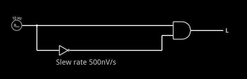
In fact, it can, but only because the circuit elements are not as perfect as we’d wish. When the input to the inverter changes, the output can’t instantly change. Part of that is due to the capacitance of the output circuit. Other delays are due to specific physical effects of whatever element implements the inverter (a transistor, a relay, or a MOSFET, for example).
Consider a time right before the input goes from low to high. The input is low and has been for a long time. The inverter’s output is high, so the AND gate outputs a 0. Now the input goes to the high or true state. The inverter will eventually output a 0, but not right away. Until it does (and assuming the time for the wire to carry the signal change is much smaller than the inverter’s propagation delay) then the AND gate will output a 1 (after, of course, its own propagation delay). This forms a basic rising edge detector. The output pulse’s width will depend on the delay through the inverter. No matter how long the input stays high, there will be just one short pulse at the output.
In real life, you’d want to make the inverter actually quite slow to get a certain pulse width out of the detector and to offset the delay of the AND gate. You might use an RC network to stretch the timing, for example. You could also use an odd number of inverters. If you were designing an IC, you could do things with the device geometry to make it slow.
In the case of the Falstad simulator (click this link to simulate the circuit), I set the slew rate of the inverter to 500uV/second. If you visualize the output of the inverter on a scope, you’ll see the output edge is more of a ramp and that is what makes the edge detector work. (Note: the simulator may show the circuit off to one side of your screen or perhaps even entirely off your screen. To correct this, select Edit | Centre Circuit from the simulator menu.)
In Verilog there is a delay statement you can use to model this kind of behavior during simulation. When you synthesize for an FPGA, you can’t use the delay statements, but the tools do know what the real gate delays are for the FPGA circuitry and will use those. You just can’t change them.
In fact, Verilog recognizes two kinds of delay: inertial delay which is the amount of time it takes a component to recognize a change and transport delay. There’s a good paper that covers how you can do different delay modeling in Verilog, but for now here’s the same edge detector in Verilog:
`default_nettype none
module edgedet(input a, output z);
reg b;
assign z=a&b;
always @(a)
 b<=#2 ~a;
endmodule
The assign statement is equivalent to the AND gate and the always block is the inverter with a 2 clock cycle transport delay. However, my point isn’t how to make an edge detector. My point is that real life delays can be exploited (although they can also cause problems).
The Case for Sequential and Clocked Logic
It should be pretty obvious that sequential logic is necessary for anything that has memory. However, you’ll find that nearly all real world designs use a specific pattern. Each bit of combinatorial logic will get its inputs from flip flops that use a clock. The outputs will go to other flip flops on the same clock. Those flip flops, in turn, will drive other gate inputs. This is known as synchronous logic.
In theory, you don’t have to do it this way. However, if you don’t you are asking for a lot more work. Consider the following scenario. For an industrial control project, you need to quickly shut power down if sensor input “B” goes high unless sensor “A” is also high at the same time. The easiest way to define this is with an AND gate fed with input “B” and the inverse of input “A” (although, of course, there are many ways to do this; that’s not the point).
Here’s a simulation of the circuit below that also has a slow inverter. If you put the switch in the down position you can control A and B separately. If you throw the switch up, then the top logic input controls both A and B (click the H or L to invert the state of the input). When A and B go from low to high at the same time, a glitch occurs on the output. If this turned the power off to the machine, it would be an error. You can find the same model in Verilog, too, if you like.
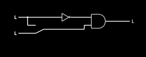
With a clock and flip flops, the slow inverter won’t matter as much. If the longest delay from input to output is shorter than the clock frequency, then the glitch won’t appear on the output. I’ll talk more about a D flip flop later, but for now just think of it is as a one-bit memory. When the clock goes from low to high, the output becomes whatever the D input is at that exact moment. At all other times, the output doesn’t change. Now if A and B are fed into D flip flops and the output goes through a D flip flop, the glitch may still happen, but it will happen while no one is looking (that is, not at a clock edge). it may be true that if a tree falls in an empty forest it still makes a sound, but a glitch that isn’t clocked into a flip flop just disappears.
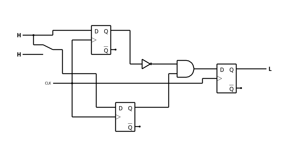 Adding flip flops makes the circuit look like the one on the right. You can see how it works in simulation (again, put the toggle switch up and go from L to H; you’ll see a glitch in the intermediate result, but not on the output). If you prefer to experiment with Verilog, you can model the same effect, although you may have to wait until we talk more about flip flops in Verilog to get the most from it. Either way, you may notice something. If the input is too short (relative to the clock) the circuit will ignore it. In general, the clock rate needs to be at least twice as fast as the fastest input you need to process.
Logic Elements
Hopefully by now, you agree that these flip flops and clocked logic are a good thing. There are lots of variations on flip flops and other sequential circuits. However, there are some generally agreed to names that cover the basic types of circuit elements you’ll need. The details, though, may vary (for example, a flip flop might activate on a rising edge of the clock or a falling edge). Other inputs might take a high voltage as a true, while others use a low voltage. The concepts, though, are the same.
To avoid confusion, I’ll use the word asserted instead of true. Just remember that while asserted often means true or logic 1, it could mean a 0 if the input is an active low input.
There are several elements worth discussing: SR, D, T, and JK flip flops. Of the four, one (the SR) often is not clocked (and is usually called a latch). The other three (D, T, and JK) have clock inputs although you sometimes see latch versions, especially of the D flip flop. You’ll see the difference shortly.
Flip Flop Signal Names
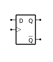 Regardless of the type of flip flop, there are a few common things to watch for. In a schematic symbol (see right), there will be a small triangle inside the flip flop’s box. This is the clock input. If there is a little circle on the outside of the box right next to the triangle, it is a negative edge
 or level clock (there isn’t one in the picture on the right). (As [Sheldon] pointed out in the comments, technically the triangle should only be present for an edge sensitive clock, but it isn’t uncommon to see the symbol used incorrectly so watch out.)
The output of a flip flop is almost always called Q. As you’ll see, the design usually produces the inverted output for free and that is represented as a Q with a bar over it. In all cases, if the Q output is asserted, the Q-bar output is not and vice versa.
You may find flip flops that have particular features. For example, a preset allows you to force the Q output to true and a reset forces it to false. A synchronous preset or reset only occurs when the clock is active (that is, on the active clock edge or level). An asynchronous preset or reset occurs immediately regardless of the clock. Some flip flops have a clock enable input. When this input is not asserted, the clock is ignored.
The Latch
Latches have a bad reputation because they are generally not used in FPGA design. At least, not on purpose. Bad coding can produce unexpected latches and these can cause havoc with FPGA tools, especially when they try to make your circuit run at the fastest possible clock speed.
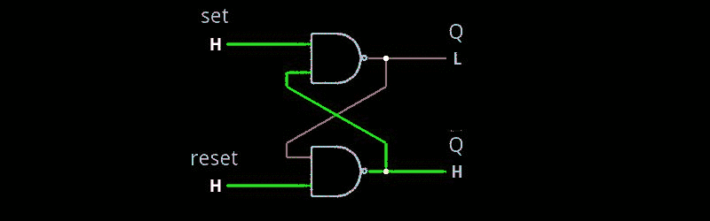
However, latches are an important building block and they are easy enough to understand. The simplest kind of latch is the SR latch (sometimes called an SR flip flop). The S stands for Set and the R stands for Reset. If you assert the S input the Q output will assert. If you assert the R input, the Q output will not assert. If you assert both the S and the R input… don’t do that. The result is undefined, which is one of the problems with using an SR latch.
The logic implementation of an SR latch is simple. It is two inverting dual-input gates (either NAND or NOR) cross connected (see below). Whichever gate you pick, you have to use it for both gates. If you use a NAND gate, the S and R inputs will be active low. If you use a NOR gate, they’ll be active high.
The Falstad simulator has an example circuit of a NAND SR latch you can pick from the example circuits menu.
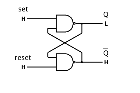
The Verilog equivalent is simple (use nor, if you prefer):
module SR_latch(input R, input S, output Q, output Qbar);
 nand (Qbar, R, Q);
 nand(Q, S, Qbar);
endmodule
However, you should not do this to actually synthesize an SR latch on an FPGA. The tools will do a much better job if your logic is all clocked. This is just a building block and just because you can model it in Verilog doesn’t mean you should synthesize it.
Next Time
Latches have their uses, although as I mentioned earlier, getting them in your FPGA can cause all sorts of timing problems. What you really want are flip flops that use a clock and that’s the topic for next time.
One of the nice things about simulations is that you can experiment easily and without fear of letting the magic smoke out of components. Can you think of a way to add an enable input to the SR latch? That is, a way to make the latch ignore the S and R inputs unless there is an enable signal asserted. There is a way, and that’s something we’ll look at next time.
If simulation leaves you thirsty for real hardware, you can always check out the video from [Dave McAnulty] below.
You’ll also want to check out the next part of this two-part series.


“If there is a little circle on the outside of the box right next to the triangle, it is a negative edge or level clock”
Er, no, it’s only negative edge.
The triangle is intended to indicate that a transition event is required, if the pin results in change when the signal is at a level then it should not have the triangle as it is an enable (it may still be driven from a repeating signal such as a clock but it is still only an enable input).
Well you are correct, although recent common practice you often see the triangle used on a level or left off of an edge sensitive input even though it isn’t technically correct. This is probably due to cookie cutter symbol libraries. I’ll add a note in the text in a bit to clarify that. Thanks for keeping me honest.
I have to admit to spending slightly more time than I should have confirming it.
Frustratingly, a ‘recommended video’, that came up after watching the one above, from an actual teaching group said one thing about it only being an enable but then proceeded anyway to use the clock edge symbol because that was what they’d cake the signal :-/
Guess it’s one of those things to watch for in any coding exercise where people name variables (don’t get suckered in by what it looks like!)
@[Al Williams] I sigh in disappointment when I see these Verilog tutorials because they’re great and I do VHDL :(
Damm had to fix my name thanks to burningfeet
The triangle inside the box specificity represents a *positive* edge triggered input. The circle outside the box represents an inverter turning the positive edge triggered input effectively into a negative edge triggered input.
Thanks HaD (and specifically [Al Williams]) for these ‘back to basics’ articles! Great info for those starting out, and even for experienced hackers it doesn’t hurt to revisit some things that you may not have done in years.
Cheers
[Al Williams], thanks for the article!
Just a note: I had no idea the Javascript version of Falstad’s circuit simulator could encode the running sim in a URL! That’s an awesome asset for web-based instruction.
Unfortunately the link appears to hardcode the screen viewport somehow. When I open the linked examples, the schematic is scrolled off the right side of the browser window with no way to center or resize; on a smartphone screen, it doesn’t show up at all.
I assume what’s happening is that the sims are created in a full-screen, wide-aspect browser window. It might be a good idea to shrink the browser window to fit the circuit before exporting the link, so it’ll render properly on small screens.
I noticed that about an hour after this posted! The quick work around is go to the View menu and hit “Center Circuit” (or something like that). Long term I will try to update them to not be on my huge monitor in the next few hours (and in the follow up).
Sorry, that’s the Edit menu in the simulator, not view. Try that.
Edit -> Centre Circuit worked, thanks!
I will try to have a better fix soon.
Ok, I patched up all the links to have the circuits closer to the corner and added a note. Hopefully that will work better.
For the record, this is my desk setup:
http://imgur.com/wwZwG2M
That middle monitor is a bit large ;-)
Umm, the middle monitor is too small. If it were were larger then you could mount the smaller ones vertically to the sides of the larger and all would fit together nicely.
Actually, I was thinking about rotating them to portrait the other day since they are as wide as the main monitor is tall. I don’t think they have that option so I’m going to have to fire up the 3D printer and build some mounts.
Quality article, thanks, will be adding this to my kid’s learning materials.
How do l save the changes i made in the circuit simulator?
@keghn, see the File -> Export as [Link|Local File|Text] options. To reopen your modified version, use File -> Import From.
You might enjoy this Digital Logic tutorial which focuses on NAND gates.