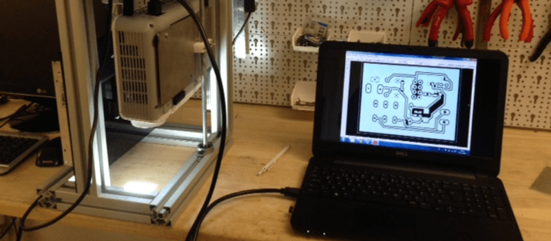
There’s so many ways to skin the home-fabrication-of-PCBs cat! Here’s yet another. [Nuri Erginer] had a DLP projector on hand, and with the addition of some reducing optics, managed to turn it into a one-shot PCB exposer.
If you’ve ever used photo-resist PCB material before, you know the drill: print out your circuit onto transparency film, layer the transparency with the sensitized PCB, expose with a UV light for a while, dissolve away the unexposed resist, and then etch. Here, [Nuri] combines the first three steps in one by exposing the board directly from a DLP projector.
The catch is that the projector’s resolution limits the size of the board that you can make. To fab a board that’s 10cm x 10cm, at XGA resolution (1024×768), you’ll end up with a feature size of around 0.004″ in the good direction and 0.005″ in the other.
For DIP parts, that’s marginal, but for fine-pitch or small SMT parts, that won’t do. On the other hand, for a smaller board, optimally one in the same 4:3 ratio, it could work. And because it exposes in one shot, you can’t beat the speed. Cool hack, [Nuri]!
When you need more precision, strapping a UV laser to an accurate 2D robot is a good way to go, but it’s gonna take a while longer.


Why DLP? Why not a vanilla LCD projector?
(Is it because of the contrast ratio?)
At a guess, it’s because with a typical LCD projector, the light source is split into three and then filtered through red, green and blue LCD panels, which probably removes much of the UV component. With a (single chip) DLP projector, the light passes through a spinning colour wheel, which has red, green and blue segments, but generally also includes a ‘white’ (actually clear) segment (to enhance the reproduction of white in the projected image), which lets the light through unfiltered.
Actually it’s the polarisation filters that block the UV. I tested it when I started building my DLP based SLA. You can get uv capable polarisation filters but they aren’t cheap. Yet for some DLP projectors collor wheel removal is necessary
UV kills LCD panels over time, so there’s an intentional UV filter coating on them – it’s not a side-effect of the polarisation.
right, and it gets even weirder – some polarizers work in the NIR while others don’t (around 850-1000nm) or have a significantly reduced extinction ratio.
For reference there are polarization rotator or nematic cells for optical assemblies and they are available for UV (see thorlabs LCC1113-A specs as an example) – so the TN cells themselves need not necessarily be the limiting factor.
If a collimated beam is used, polarizing beam splitters might be an option – unfortunately they are quite expensive.
Interesting. I was wondering why my polarizing ND filter didn’t work with my infrared camera (650nm ish).
How about hacking a laser printer to print directly on the PCB ?
check this :
http://www.instructables.com/id/Modification-of-the-Lexmark-E260-for-Direct-Laser-/
AFAIK laser printers use electric charge to print on materials, so printing material needs to be an isolator.
My suggestion was to use the laser and rotating mirror to directly write on the photoresist layer, and get rid of all the electric charge stuff.
No, there’s nothing stopping a conductive material from building up a static charge; it just needs to not be grounded. You can attract charged particles to a charged metal plate no problem.
Hmmm… but the charge would distribute evenly over the whole copper layer, so it’d end up with an even cover of toner…
not quite – the process is –
image drum is charged evenly over surface
laser removes charge from drum where page is to be left white
drum is rotated over toner and toner sticks to still charged areas of image drum
drum is rotated over/with paper with a charge behind paper to attract toner onto paper
paper then goes through fuser which is hot enough to melt the unfixed toner onto the paper
I may have this wrong and it may be that the charge is only passed to the image drum where it *has* been pre-exposed to laser
feel free to correct me
http://www.instructables.com/id/Making-flexible-PCBs-with-a-laser-jet-printer-or-c/
The laser printer drum is where the laser scanning, high voltage imaging take place. The resulting toner is transfered to the paper or whatever you have and fused by the high heat.
These days, the drum and toner on consumer printers are sold together in a cartridge.
http://www.explainthatstuff.com/laserprinters.html
They are sold together for cheap(er) printers, the office and printhouse behemoths are almost always separated, as they use a transfer belt the photosensitive drum doesn’t come into contact with the paper, so it lasts much longer than one toner cartridge…
We used to have a Qume printer, it had a photosensitive belt… and separate toner cartridge.
(FYI)
This has come up on hack-a-day (long time ago). I had an old laserprinter laying around and tested this exact question by feeding it a sheet of paper with some alu-foil taped on to it. If I remember correctly, delivering the ink worked, but was not fixated to the foll because the printer did not get the foil hot enough.
http://hackaday.com/2012/08/09/exposing-pcbs-with-a-home-made-laser-printer/
This one is really neat! I can’t believe that I forgot to link it into the article.
Everyone click here. (Video is in German, but docs are in English.)
Try the OKI series!
I own a C321 and it does deliver VERY sharp points AND has an almost straight feed-line when you open up manual feed and the back-tray. I print on 370g/srm paper with it… Also that color printer is way below € 200,-.
Modding a monochrome version to accept PCBs should be doable.
Too many modifications needed I believe. An Inkjet would be almost there, save for the type and amount of ink needed since copper would not absorb it.
Anyone find anything on filling an inkjet tanks with negative or positive etch resist? OR I’ve a BETTER idea for Inkjets.
I’ve a Inket Printer that has a CD-ROM Tray… For a full page it specs @ “Maximum Resolution Color: 9600 x 2400 dpi, Black: 600 x 600 dpi” So at best color conversion it comes to 94.4882 dots per mm x 377.9528 dots per mm for A4/Letter AKA 8″ by 10″
The CD try handles a standard 120 mm (4.7″) BluRay/DVD/CD.
Sadly, fullspectrumengineering.com/pcbinkjet.html has had everything out of stock for a long time now.
Has anyone attempted to take a UV Laser Diode something like:
http://www.qphotonics.com/image.php?type=T&id=763
and place it directly INSIDE an Inkjet cartridge?
The cartridges themselves have LEDS indicating they ARE getting power from the printer.
http://www.steves-digicams.com/2005_reviews/ip5200/ip5200_carts.jpg
I’m theorizing mirrors and prisms in the printer head might NOT be needed as enough of the light should bounce around and end up out of the printer head.
Any takers on the idea? $99 printer?
if i recall, most inkjet printers use an array of print nozzles on the cartridge, so having 1 single beam of light emitted from the cartridge probably wouldn’t work. this article might be worth checking out http://hackaday.com/2013/11/02/perfect-pcbs-with-an-inkjet-printer/
Sadly, I’d want to keep from having to buy toner. The 1st comment is spot on.
I want to do AWAY with BOTH the toner dust AND inkjet ink!… Why would 1 beam be not enough?
Print same image 2 or 3 times.
Also you could work with positive resist or negative resist coatings quite easily? Just invert the image color.
an HP 51640M cartridge has 136 nozzles. you would lose a ton of resolution, you would be better off ditching the cartridge altogether, mounting the laser facing down, and using your own electronics to modulate and scan it across at a lower speed where you can precisely control everything.
I’m considering doing a Logic Analyzer dump with some 32 gauge silver wire, and record the traffic from carriage to head. Then chopping up the cartridges and fitting in the UV diode, resistor, etc and coat the cartridge with black appliance enamel so no extra uv gets out. Then throw the details to a teensy 3.2 mounted on top of the rig. “yeah yeah tanks are 99.7% full and fire away the data stream.” I don’t know the print head clock speed so… some research into that..
You could scan the board under the projector with a simple gantry while the graphics scroll on-screen to expose a larger board.
Yes Dax,
That is what I want to test next. This way very big boards can be exposed. 20 sec is more than enough So process can be fast
If you moved the projector closer (to make the smallest feature size even smaller or allow for better compensation/aliasing when moving), does the increased brightness compensate for the extra time needed to scan over a board to ‘re-gain’ area lost in moving closer in the first place?
use Computer Vision optical alignment!
and at the end, put a tank with the developer and automatically drop the pcb there.
That’s an awesome idea. Combine the XY gantry of the UV laser with the speed and ease of using the DLP.
I want to see that done! GOGOGO!
been there, done that. When you put a little more effort into it, it’s called maskless step-and-scan lithography.
Here’s the path I took and why I gave up at some point: Several resists are rather insensitive to light so the 420-480 nm region is only 30 downto 10% as effective as an exposure at the peak sensititivty (360 – 400nm).
All the optics that came with the four DLP beamers I took apart on that journey are not compatible with 400nm and the resolution just gets worse when you add a spacer or bellows behind the lens to reduce the image size in an effort to improve resolution. These projection optics are designed for basically an infinite-conjugate optical path. For what should basically be a relay lens the construction ought to be symmetrical.
I tried an EF 50 f/1.8 lens with acceptable results and an EF 100 f/2.8 USM macro (which goes down to 1:1 ratio) but the latter significantly reduces the light output.
There are more catches: some projectors couple in the light with a prism which shows pronounced fluorescence and attenuation and so do some elements in the light homogenization path (caleidoscope rod and lens array plates). When you toss these and add a 5W 395nm emitter like I did, you’ll most likely end up with vignetting (radial variation of the exposure time) which has to be compensated in software.
So to wrap it up:
– for good results a small optical bench / cage system has to be built, most of the optical elements have to be discarded and re-done for UV
– 5W UV LED star emitters are a good starting point
– HID lamp emulation is straight forward in most models (two or three opto couplers are used, one returns a power-good signal. Emulating the HID ballast can be as simple as putting in a jumper, one model (IBM) required a more sophisticated delay circuit because the controller does some sanity checks and PWMs the ballast control signal
– haven’t found a workaround for the colour wheel BLDC driver. The colour wheel tacho signal is absolutely mandatory because the DLP signal generation has to be in sync with it. Tacho signal can be derived from BLDC PLL reference clock in some models.
– a precise XY positioning stage and a camera are a very good idea to automate alignment (double-sided PCBs)
But yeah, as with most of these projects… you can get away with much less effort when you’re willing to accept partial success.
Here is another step by step…
https://hackaday.io/project/2105-sedgwick-the-3d-dlp-resin-printer/log/5505-print-your-own-pcbs
I tried that a few years ago. It worked quite well with my standard BenQ projector. But I actually never really used it afterwars as I have a PCB mill now. But I like the Idea!
I’ve been using this method for quite some time now. Very convienient. For my Viewsonic HD projector it’s less than a minute to expose. Only problem: resolution isn’t that great. Below 200 um is unreliable. Plus, there is always some distortion making double sided close to impossible for fine structures.
Several months ago I was looking a bit into what it would take to make an extremely low density IC that did away with physical masks for the lithography process. I thought about projectors and went to TI’s site to see what their highest res DLP array was just to find that one of the stated uses for their DLP chip was PCB photolithography. I wonder if there’s any commercial hardware out there that actually uses it.
yeah but its patented…idk how the fuck they got a patent on such a bloody obvious idea so late in the game… or a patent that requires using tis patent. i fucking hate patents. long story short it exists but you wont find it for sale in the us or strong allied countries. I read the same article but followed up with google
Cool, I’ve got an old 1024×768 DLP languishing in the closet… Wonder if this’d be good enough for SMD on really really small boards. (I don’t need 10x10cm, that’s for sure!)
Thought I should share this. Photolithography using a projector:
http://pages.pomona.edu/~dmt04747/Pubs/MasklessLithoAJP.pdf
…and a microscope.
Kind of makes me wonder how far away DIY ICs are.
I always wondered if someone could adapt LightScribe technology to print photoresist onto CD-shaped copper clad boards…
Swap out the laser diode for a UV and expose the resist layer on precoated boards.
Hay una gram cantidad de errores en las suposiciones hechas anteriormente.
1)- Para obtener una resolución (minima necesaria ) de 600 ppm, con un DLP de 1024×768, la superficie a proyectar sería de 32 x 43 (mm), o sea, una superficie muy pequeña para cuanquier PCB.
2)- Para obtener una imagen enfocada de esa superficie se hace obligatorio modificar la óptica del proyector. Generalmente, la menor superficie enfocada de esas opticas es de unos 300 x 300 mm. La modificación de estas ópticas es obligatoria, pero sencilla.
3)- Los proyectores DLP domésticos usan una óptica denominada atelecéntrica (non telecentric), lo cual provoca irremediablemente una imagen trapezoidal (keystone). La resolución óptico-mecánica de este problema es económicamente imposible; por lo que su resolución es obligatoriamente digital, mediante una reconvolución por software de la imagen, con la consecuente pérdida de resolución.
4)- Las ópticas notelecéntricas generan además aberraciones esféricas, por lo que la superficie útil real de la zona proyectada se reduce a un 70 %.
CONCLUSION: Es posible la fotolitografía DLP para fabricación de PCB, pero pasa obligatoriamente por una tabla X-Y en donde se realizarán fotoexposiciones de aproximadamente 15 x 15 mm hasta completar la superficie. Algo bastante distinto a lo que se plantea inicialmente.
Próximamente publicaremos los resultados de un primer prototipo funcional.
Grupo Patel
Mostly-accurate machine translation:
There are a gram of errors in the assumptions made previously.
1) – To obtain a resolution (minimum required) of 600 ppm, with a DLP of 1024 × 768, the surface to be projected would be 32 x 43 (mm), that is, a very small surface for any PCB.
2) – To obtain a focused image of that surface it becomes mandatory to modify the optics of the projector. Generally, the smaller focal area of these optics is about 300 x 300 mm. Modifying these optics is mandatory, but simple.
3) – Domestic DLP projectors use an optics called non-telecentric, which inevitably causes a keystone. The optical-mechanical resolution of this problem is economically impossible; Reason why its resolution is obligatorily digital, through a reconvolution by software of the image, with the consequent loss of resolution.
4) – Notelecentric optics also generate spherical aberrations, so that the real useful area of the projected area is reduced to 70%. CONCLUSION: It is possible DLP photolithography for PCB manufacture, but it is mandatory for an X-Y table where photoexpositions of approximately 15 x 15 mm will be done until the surface is completed. Something quite different from what is initially proposed. We will soon publish the results of a first functional prototype.
Patel Group
I did it with an LCD screen
see: https://youtu.be/hczjN9er9TI