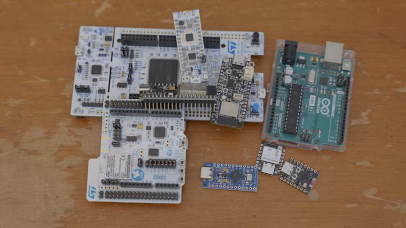
It’s fair to say that there are a lot of development board form factors for MCUs, with [Tech Dregs] over on yonder YouTube on the verge of adding another one to the pile, but not before he was having some serious thoughts on the implications of such a decision. Does this world really need another devboard with the ubiquitous 2.54 mm (0.1″) pitch pin headers, all so that it can perhaps be used in the same traditional 2.54 mm pitch breadboards?
The thought that [Tech Dregs] is playing with is to go for something more akin to the system-on-module (SoM) approach that’s reminiscent of the Raspberry Pi compute module form factor. This means using a 1 mm pitch for the headers and castellated edges in case you want use it as an SMT part, while breaking out many more pins of the onboard ESP32 module in far less space.
Obviously, the main advantage of this approach is that much like with compute modules you can leave most of the tedious cheap stuff on a carrier board, while the expensive to manufacture components are on a self-contained module. Meanwhile with the much finer pitch on the SoM contacts it’d straddle the divide between a 2.54 mm breadboard-capable devboard and a fully custom PCB, while making any mistakes on the carrier board much cheaper to redo.
The counterpoint here is of course that something like an ESP32 module is already a module with a finer pitch, but if you need more than just what it offers, or you want to use an STM32 or RP MCU across boards it could make a lot of sense.
Having 1 mm pitch breadboards would honestly also be rather nifty, natch. That said, what are your thoughts on this matter?


Much finer pin pitch is 100% guaranteed to be more fragile.
And one thing that designers should always have in mind with dev-boards, is to keep the design idiot-resistant.
And I know some pearl-clutching troublemakers are gonna lose their shit over me insinuating that people unintentionally damaging dev-boards are all idiots, well keep this in mind:
I’ve damaged dev-boards by not thinking things through, and my immediate thought upon realizing the damage was always “wow, I’ve been a idiot just now…”
letting the magic smoke out the first time is a rite of passage. doing it repeatedly, that’s stupid.
idk it’s just a matter of time, not stupidity. The human brain doesn’t improve efficiency, and if the last ten years of my life are any indicator, it degrades rather than improves over time. Really if you are lucky enough to retire at 64 and start doings these little projects as a hobby (maybe even with a hope of developing something commercial) “Idiot-proof” becomes a necessity.
by repeatedly i mean one after another in rapid succession. eventually you are going to screw up again, that’s just a fact of life. frying a board every few years is nothing to be ashamed of, going through ten in a week on the other hand.
The person who’s never f*cked up is the person who’s never done anything.
When you’re developing stuff and there’s modules, wires, probes, etc. all over the place it’s really not hard for even experienced folk to accidentally short a pin, plug the wrong power supply in, etc.
We’ve all toasted dev boards that’s for sure :)
I think the biggest issue is people using dev boards for final solutions in places they shouldn’t. Sure they work but honestly, the likes of the Megasquirt v2 and then v3 became the epitome of this. If you wanted some of the options you had boards in 2.54 pin headers to match motherboards with the original processor footprint, with daughterboards bolted on elsewhere flying leaded together. It worked, providing you didn’t get too much vibration. At some point you shouldn’t be using a dev board and should be understanding how to convert the design to a proper self contained one. (before you say it, i know the megasquirt were not technically dev boards, i was more using it as a demo of stacked nonsense connectors)
“Idiot resistant” is a great way to describe it! Because achieving “idiot proof” is impossible.
Yea, no design was going to prevent me from running 24v 3a into a little Arduino because I was tired and had a terrible wire coloring scheme.
Frying boards is a fact of life.
i’ve got no problem with new dev boards dave on eevblog reviews many on his mailbag. My biggest gripe with them is that the designers who make them design them specifically for a project they have in mind so they are single purpose dev boards instead of actual dev boards if that makes any sense. Anyway the more the merrier and if you don’t like it to bad i say.
you can do a lot just wiring breakout boards together with you microcontroller platform of choice. get around pcb etch entirely with a good crimp set. i know at least once i put pull up resistors into a wiring harness. its like lego.
I primarily use breadboards but i do like to keep an eye out for dev boards especially ones aimed at motion control. But again there is the issue it really isn’t a pure dev board like you would have on a breadboard, but more of a breakout board with motion control in mind and everything else is an afterthought.
In my experience and field of expertise, wiring modules together instead of making custom PCBs is what all the luxury brands are doing these days.
So… a dev board you can’t use without a custom pcb?
Not very prototype friendly.
breadboards are kind of limiting when you get to the advanced stuff. you can have cheep pcbs made, but i just cut of some fr4 stock and get out the engraving tools. chem etch when i have the stuff. no budget hacking with materials i already have is kind of my thing.
theres always something better, but my go to is still a knockoff sparkfun pro micro (atmega32u4). just because im very familiar with its datasheet. does 90% of my projects just fine. if i was more knowledgable about an stm32 or esp32 id probibly use those, but ive never really needed that much cpu power for the stuff that i do (mostly usb control stuff, joysticks and the like). i have other boards, like the due at the back of my desk i dont remember buying, several esps, an stm32 and a mojo fpga board, but ive never needed them.
It starts with only two different types (maybe three) at the beginning. There are 3 boards which have the horrible arduino pinout. Usually big empty PCB, that fits with nothing else. The other type has the standard 2.54mm pitch, and fit in a breadboard. And this is great for prototyping And that is what those dev boards are for. The third type has the added castellations that also make it solderable as a module.
For me, it’s pretty simple. A devboard is for getting to know a system, and also for quick projects. and the 2.54mm pitch is just perfect for that. Not only for breadboards, but also for more permanent solutions on matrix (vero) board. If it has a difficult to use pitch. I won’t start with it. Simple as that. And as a result I would not get to the point of the intended use.
What I do see as an upgrade is to use an 1.27mm pitch. This way you can maintain breadboard (and matrixboard) compatibility, provided you can skip the odd (or even) holes, so power and important pins must be on the 2.54mm grid. This probably wont fit with the big holes needed for the square header (dupont) pins, but there are also much thinner round pins on strips with a 2.54mm pitch.
Overall, I’m all for nice round metric numbers such as whole mm, but those development boards it’s (unfotunately) simply not practical.
Two other improvements I would like to see more: More ground pins. The Raspi uC boards have a GND pin every 5 pins or so. That’s (probably) a significant improvement for signal integrity and EMC. The second is 4 layer PCB’s with internal GND planes. The Nucleo boards from ST have it. The cheap stuff from china does not. The original “Maple Mini” apparently also had 4 layers, but the clones did not. And the cost is quite minimal. Once development boards get into the 1000+ boards, the price difference is less then 50ct.
Little quiz:
You you had a choice between an EUR 4 devboard with a 2 layer PCB or the same board for EUR 5 but 4 layers and internal GND plane, which would you buy? “cheap”, “quality” or “both” to experience how big the difference is?
Cheap first, of course, the try the better one.
Ideally a prototyping board is compatibel with a breadboard, so 2.54mm pitch and has a cousin – electrically compatible – with castellated 1.27 or 1.0 (I really don’t care, the pcb world is mostly frozen in the 0.1 inch-era) for small scale- or pre production series.
Arguably the smaller version don’t need advanced on board power supply and/or usb connector.
While I love the versatility of the rPi, it’s just an average board with an exceptional community (nothing else can touch, besides the Espressif community). That’s not a dis, just honesty.
I really like the Compute Module and it is nice to see it becoming more of a (de facto) standard.
My work’s use case is dual-Ethernet (real Eth, not USB dongles), being able to do router prototyping in a familiar (still a Pi, but always evaluating others) environment. Having robust carrier boards is MUCH better than trying to find “hats”.
Hats are hot garbage for real work. The worst thing is if you need 2 of them (ewww, when it even works).
I’d love to see tiny micros start using the carrier board format.
Do we need more dev boards? HELL YES!!!! Keep the 0.1″ pitch? Again, YES!!! There are hundreds of cheap breadboards out there, with hundreds more solderable proto boards with that pitch. Yes, it’s a remnant of through hole parts with leads that fit perfectly in the holes. Between pluggable, solderable and wire-wrappable they are easy to use, cheap and readily available. What else do you want for your prototyping?
Go to a smaller pitch and you can’t plug it into anything available, the leads don’t work in those 2.54mm pitch devices. Surface mount? Ever tried to plug a SOT-32 into a breadboard, it doesn’t work. But there are places that will custom make a PC board on the cheap for your project.
As a professional engineer, my breadboards and these dev kits allow me to explore any new micro or component that comes out quickly with minimal difficulty. Otherwise I have to wait 2 weeks for a board to be delivered then take time building the board. That’s a great plan for a dedicated board, but a dev kit I can reconfigure and keep working on new designs with a flexibility that I need.
As a hobbyist and ham I have a cheap, flexible platform to build whatever project I want. It affords me an affordable way to try out new and different micros or other new devices in an evening without creating a one-off PC board and waiting on parts and boards to arrive.
As long as new micros and devices keep rolling out, ABSOLUTELY keep making dev boards!
Designing for breadboards means – accepting breadboard limits. The most obvious one being: SPEED.
I’ve never seen an official max clock rate for 0.1 inch connectors. I’ve ALSO never seen an ADC use that connector, running at higher than 60MHz.
Some microcontrollers use 120MHz or higher. Breadboards, and 0.1 inch connectors, are NOT appropriate at that speed.
Even modest improvements in (constant) trace width, and and matched length, should increase effective data rates significantly. If that means castellated boards with 1mm pitch, so be it.
The 0.1″ headers can handle fairly high frequencies. Motherboards run 480 mbps USB signals over them. That’s using low voltage differential signaling and twisted pair cable though.
Running TTL signals at more than a few MHz on a solderless breadboard with long jumper leads going everywhere is asking for trouble.
Lol, that’s not how downvoting works on youtube. You just guaranteed they’ll show back up in your feed. Nice one!
Follow the money (and development speed). Making the same boards is much cheaper than custom + well documented. The custom boards are not prototype dev boards. These are 2 different things.
I like 0.1″ pitch (2.54mm, pfft)…but the fact of the matter is that for a lot of projects i only wind up using a handful of the I/O pins anyways. I need them all exposed because i don’t know which ones ahead of time…but if i only need to make a handful of connections, i usually don’t mind hand-soldering like 28awg wire wrap wire. But i also usually don’t mind the board being big so i’ll be buying the 100 mil spacing :)
I work an entire semester with undergrad design students, and it pains me to see that the Chinese manufactured ESP32 boards have zero protection against any mistake. It seems like the boards are made so fragile that the purpose is to sell more.
Yes, we do need new dev boards because we need to support specific project goals.
It’s not just the chinese. uC breakout boards very rarely have any I/O protection. On top of that, the newer boards are much more fragile then the old 5V uC’s. And when you get into faster logic (FPGA’s, Linux boards) it gets even worse. More then 2V on an I/O pin and poof! you let out some magic smoke.
Usuallly you only see I/O protection on boards that are not really development boards, such as the EUR 8 Saleaeaea clone Logic Analysers. or programmer dongles for other boards.
I disagree. The only reason for such a dev board that you envision is ‘education’. How many people need education, and for how long? After the education is done, people need to use the boards in projects. And then they should be small, single-sided, and easy to solder onto a carrier board.
I’ve actually designed boards where I just copied the entire circuitry of the dev board into my design because the original dev board’s form factor was just too big. If that dev board would have been as small as possible, and would have been single-sides SMT, I would have just soldered it onto my carrier board.
I tried to do the same with a Raspi Pico once, but found that my board would not be smaller than when I would have just soldered a Pico onto my board. So to me the Raspi Pico is a great example of a good dev board.
Maybe they should make one without the USB, to make it smaller. But it’s actually a good thing because it gives me a ‘free’ power supply and communication capability for the rest of my board.
Espressif should take note and design a WROOM and WROVER board with the USB built in. And maybe add a beefier power supply that supports USB-C power delivery and can supply more than just 3.3V 500mA. Although I’ve never had the need for more current (yet).
Also, a lot of my designs use mixed 5V and 3.3V. I usually take the 5V directly from the USB, but that could cause noise on the 3.3V that I regulate from that same 5V. So a separate design with buffered 5V and 3.3V would be a nice feature. Also some way of knowing if I go over the power budget of either the 5V or 3.3V would be nice.
Not sure what kind of protection you expect. I feel like every time I have looked, GPIO, for example, is not protected beyond what’s built into the SoC. Like, on raspberry pi, or pico, or STM32, etc, i don’t think i’ve ever seen anything like optoisolated IO or external protection diodes or anything like that. In fact, it’d be hard to come up with something that makes it much safer that doesn’t also interfere with all of the different analog / high-impedance input sort of modes that the GPIOs have. I guess I do expect most things to at least survive reverse-connecting the power supply but even that, i don’t know if i’d be too surprised if I burned something out that way!
The thing is, i’ve burned out a few IO pins on the PIC12 (DIP8 5V). And looking back on it, i think on the PIC16 too. I am not sure how it was happening but i got superstitious about those after a while. But i’ve never had any trouble with 3.3V IO on these ridiculous modern ARM SoCs. Maybe i’ve just been lucky. I’m always expecting to kill things with ESD or careless connections but only the classic PICs ever got injured.
feather size is ok, I like OrangeCrab
I seem to recall the same question when ESP devices were introduced. I think the answer is obvious.
Lately I have been using some newer STM32H750 boards and some others. Any of them with dual row pin headers can’t be used with the wireless breadboards. I can not see any reason to keep using 0.1″ headers on these. 2mm headers, as opposed the the 2.54mm, are surprisingly more compact and nearly as strong. But what would be better?
Once you get into boards like that, (With 100 or so I/O pins) then they don’t fit a breadboard very well anymore, but I still very much prefer the 2.54mm pitch. After the DIP / Breadboard compatible format, the next best thing is for dual row IDC connectors / headers. It’s still relatively easy to breakout an IDC to a breadboard, and it’s easy to use dual row headers on Vero / Matrix board. And the board is going to be a bit bigger anyway, so there is hardly any benefit to make the connectors smaller.
A dev board should be cheap. Period. All those through-hole components are expensive. So a dev board should not have any.
They also add to the height of the board and prevent the board from mounted flush on another PCB. Which is just another reason to forego on them.
Dev boards with through-hole components only exist to entice novices to buy them. But for how long is anyone a novice? Anyone who really wants to go into MCU development, instead of trying something and then moving on to the next interest, will not be daunted by having to solder a few wires onto a dev board. Or use clips instead of dupont wires. Or build a carrier board, if there is any reason to do that (I’ve never found any).
This is my (quite strong) opinion. :)
My dev boards, if not fried, become integral to the final product in some cases. Those one off designs that only apply to personal applications. But should I design a device for a wider audience then the dev board is reserved for the a prototype mcu, and not for a production run.