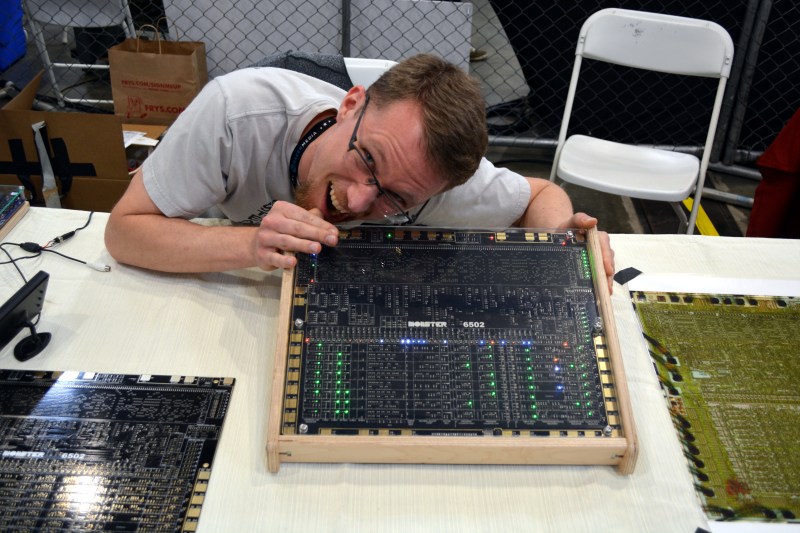
I made a bee line for one booth in particular at this year’s Bay Area Maker Faire; our friend [Eric Schlaepfer] had his MOnSter 6502 on display. If you missed it last week, the unveiling of a 6502 built from discrete transistors lit the Internet afire. At that point, the board was not fully operational but [Eric’s] perseverance paid off because it had no problem whatsoever blinking out verification code at his booth.
I interviewed [Eric] in the video below about the design process. It’s not surprising to hear that he was initially trying to prove that this couldn’t be done. Unable to do so, there was nothing left to do but devote almost six-months of his free time to completing the design, layout, and assembly.


What I’m most impressed about (besides just pulling it off in the first place) is the level of perfection [Eric] achieved in his design. He has virtually no errors whatsoever. In the video you’ll hear him discuss an issue with pull-up/pull-down components which did smoke some of the transistors. The solution is an in-line resistor on each of the replacement transistors. This was difficult to photograph but you can make out the soldering trick above where the 3-pin MOSFET is propped up with it’s pair of legs on the board, and the single leg in the air. The added resistor to fix the issue connects that airborne leg to its PCB pad. Other than this, there was no other routing to correct. Incredible.
The huge schematic binder includes a centerfold — literally. One of the most difficult pieces of the puzzle was working out the decode ROM. What folds out of this binder doesn’t even look like a schematic at first glance, but take a closer look (warning, 8 MB image). Every component in that grid was placed manually.
I had been expecting to see some tube-based goodness from [Eric] this year. That’s because I loved his work on Flappy Bird on a green CRT in 2014, and Battlezone on a tube with a hand-wound yoke last year. But I’m glad he stepped away from the tubes and created this marvelous specimen of engineering.


Now the question is, who do we talk to about dis-integrating a 6522 VIA?
All you need for a computer is some RAM, ROM, a 6502, and a VIA. RAM and ROM are easy to dis-integrate, so the only obstacle for a completely dis-integrated ‘modern’ computer is the VIA.
A RRIOT chip would do it. I think all these chips are about the same size, perhaps similar transistor count(*) but differing complexity. (*) Except ROMs are very dense.
If you dis-integrated a pair of 6530 RRIOT chips, some 6130 SRAM chips, a 556 dual timer, a 311 comparator, a 565 PLL and a bunch of TTL chips you could build a discreet-transistor replica of the KIM-1.
I know of a couple even simpler 6502 computers than the KIM: the Jolt, and the OSI 300. See
http://www.old-computers.com/museum/computer.asp?c=875&st=1
and
http://obsolescenceguaranteed.blogspot.co.uk/2015/09/osi-300-replica-mini-mini-6502-front.html
But can you do anything with them? A KIM-1 was a serious computer, I learned to program on it. It even had a serial port, so you could attach s much more expensive terminal, the monitor would even adjust. People expanded it tremendously, I’m pretty sure someone added floppy drive.
Various articles showed how to set the data bus to a “NOP” o the CPU would advance the address counter, so RAM could be loaded directly, doing away with a monitor in ROM, or a complicated front panel. The 1802 made this easy, but I’ve seen articles along this line for the 8080, the 8085 and the 68000. I never saw this directly for the 6502, but Don Lancaster’s “Cheap Tv Typewriter” scheme used this except he jammed the NOP onto the data but to advance the address counter to cycle though the RAM to display it on screen.
So this would bet all those diodes needed to put a monitor in ROM.
Michael
There’s a 22 megapixel image of a 6522 VIA at
http://www.visual6502.org/images/pages/MOS_6522.html
if anyone wants to get busy tracing polygons…
That is beautiful. My phone doesn’t like scrolling around 43MB, but I sure do. : )
So at what point does this chip qualify as open source?
Oh, and why do they keep Eric in a cage?
Can we have “like” buttons here?
That’s the standard punishment for perverting “STEM” to include arts…
Did he get all the bugs right? There were some little oddities, and if he got them “right” it’s probably a better reproduction than if they are “fixed”. (I seem to recall that at least one bug was fixed in the cmos variation).
Michael
If it is a transistor-for-transistor replica, it should have the same bugs. I know of one: in an indirect addressing mode, if your pointer spanned two bytes on a 256-byte boundary, the processor would take the upper byte of the pointer from the correct address, but the lower byte would come from the first byte of the existing 256-byte page instead of the first byte of the next page. (Probably using wrong terminology; it’s been a LONG time since I’ve looked at the 6502.)
We already know that it’s not as capable as the original chip, due to stray capacitance on the long traces. I suspect that that effect, and the slower clock rate it implies, kill a lot of the weirder 6502 tricks.
Not really. The design came from Visual 6502, which decapped and reverse engineered the original chips. It may not run as fast due the capacitance issues, but it should have all the instruction anomalies of the original.
So what specific MOSFETs is he using? I’m especially curious about the body-available 4-terminal one…
ALD1106
Very nice!
To me, this can only be called a masterpiece,
It has that special something to it that makes it go from FETs and LEDs to a work of art, and is worthy of being a in a museum or art gallery.
Eric Schlaepfer, you are a master hacker.
Please, please, please, please, please, please offer this in kit form! Even if it’s out of my own price range, there are many other hobbyists and enthusiasts who would sell their immortal souls (well, I wasn’t using it…) for a chance at building/owning this amazing piece of electronic art!
What would the kit be though? You and a bag of surface mount components?
I think it simply must be pick-and-placed. So then what we’re really talking about is a Single Board Computer…. err, a Single Board Processor.
In summary, yes I think many people would like to own it, but does anyone really want to do the soldering themselves?
Also, I totally agree with [Mike Field] from above when he says “Eric Schlaepfer, you are a master hacker.”
I’d hand-solder it. It’d be like a normal person doing a 5000 piece jigsaw puzzle. I’d love to get my hands on a kitted monster.
I agree with John W. It would be like mediation with a soldering iron.
Half an hour a night would most probably do my blood pressure a world of good… not to mention my SMD skills.
Like the others said, I’d hand solder that monster, just for the challenge and the fun of it.
I think a proper kit for this would be the board with no components attached (I’m sick of kits that assume that people can only solder through-hole), and all components in decently sorted and labelled bags, with the surface mount components still in their carriers. A few spares of the less expensive components would also be a good thing.
Also, I think we all agree with [Mike Field’s] statement. It’s spot-on.
components place manually ?! without losing your hair ? insane … lots of respect, love it.
It’s actually not that bad of a job to do. My first ‘real’ job I got after I got my EE degree was for a small engineering company who made small series (<100 pcs) of PCB's by hand, because the setup costs of a professional assembly line would be to high. All boards were SMD with parts in 0805 or smaller. After a bit of practice, it's actually very easy to do, in fact I used to do board assembly to clear my head whenever I got stuck during a hard debugging or board routing session :) I kinda laugh every time I read a magazine that states that SMT 'killed' the electronics hobby, it did not, cheap computers did.
I fully support this kind of pornography on hack a day.
This not only wins the Internets, the jury is still out on whether it needs to give them back. ;)
===Jac
That’s cool and I appreciate the effort that has gone into building something like this but how do these bright minds that make these wonderful creations eat, pay the mortgage, buy the parts and all that other stuff that keeps us ticking over in the conventional part of the world.
Eric’s time spend, by any sane person’s criteria, is ridiculous. So I wont be putting up or shutting up. However, it would be really cool to see a discrete CMOS design!
I do have a Neoden TM245P in the basement and a dangerous susceptibility to being pulled down rabbit holes on projects. I could be persuaded to do a run; if allowed of course.
The fold-out looks more like a spreadsheet than a schematic… Till you zoom WAAAY in.
If you really want to see something confusing then you should try to read a timing diagram of some telefon relais register if you have the chance to. I used to service them, and those folders of diagrams thankfully stopped haunting me. Example of such a relais field: http://www.bayern-online.com/v2261/artikel.cfm?DID=203&Product_ID=27120
How does the physical layout of this compare to the original silicon?
I *believe* the layout generally follows the floorplan of the original, with each function in roughly the same spot. I say this only having eyeballed the various photos of the MOnSter 6502, and overviews of the NMOS 6502 from the Visual6502 folk. I spot-checked the pin ordering of the pads, and that seems to match. (That includes the not-pinned-out VMA signal!)
Obviously, there will be differences due to the different ratio of transistor size to wire size, the wildly different transistor _shape_, the addition of der blinkenlights, and other vagaries necessary to bring this into a model this size.
I guess Eric will have to speak up on the actual details. I’m just armchair quarterbacking from a great distance. (And still trying to pick my jaw up off the ground.)
If only we could teach HAD authors that it’s is a contraction of ‘it is’ and not a possessive of it. Otherwise a nice article on an awesome project. Looking forward to the availability of the boards for this.
Now do it through-hole :p
Do it dad-bug style. Here are some examples.
(WARNING: Terrible website design. Somebody please tell me why people do this!)
http://www.hoofbags.me.uk/geekiestuff.html
People do it because it works and works very well.
Haha, I meant the terrible website design. I love dead-bugged circuits! :D
That page loaded nearly instantly for me. I prefer dark-on-light color schemes, but I like the design a lot more than a lot of modern pages.
made my day
PS: 18+ nudity; excessively view-able circuitry, viewer’s discretion advised.
At 4:55 the guy says “pull-up TRANSISTORS. Is there such a thing? I’ve heard of pull-up RESISTORS, but never TRANsistors.
Pullup transistors are precisely what NMOS gates have. The 6502 used depletion mode NMOS transistors as pullups.
http://visual6502.org/wiki/index.php?title=NMOS_Depletion_Mode_Transistors