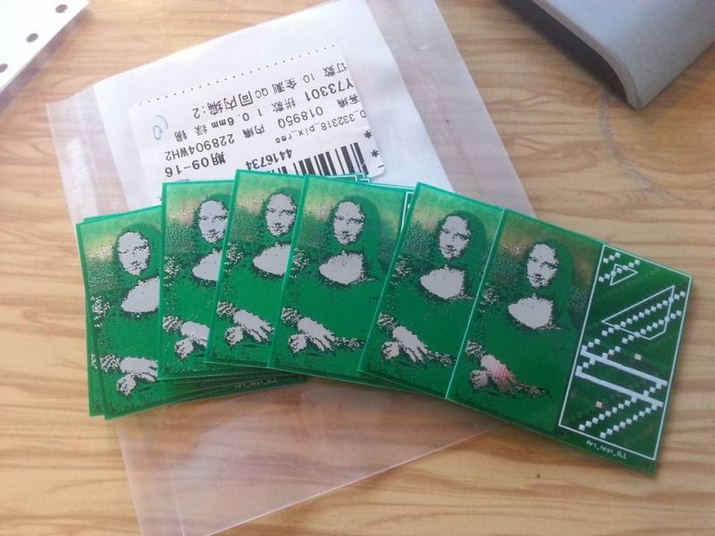
Many of us have held a circuit board up to a strong light to get a sense for how many layers of circuitry it might contain. [alongruss] did this as well, but, unlike us, he saw art.
We’ve covered some art PCBs before. These, for the most part, were about embellishing the traces in some way. They also resulted in working circuits. [alongruss]’s work focuses more on the way light passes through the FR4: the way the silkscreen adds an interesting dimension to the painting, and how the tin coating reflects light.
To prove out and play with his algorithm he started with GIMP. He ran the Mona Lisa through a set of filters until he had layers of black and white images that could be applied to the layers of the circuit board. He ordered a set of boards from Seeed Studio and waited.
They came back a success! So he codified his method into Processing code. If you want to play with it, take a look at his GitHub.


I’m still Processing his techniques, but I think I’ve finally seen the light.
I’d like to see educational PCBs with several layers of silkscreen in different colours. Red for power, black for ground – not just for wires, but the traces as well. There’s no reason that it has to be always green and white.
It can be done. Look at adafruit’s permaproto. You just need a boardhouse that is willing to do this.
I had a friend (since passed), a number of years ago who had his own PCB house, and he had a wonderful marsh scene done as a fine line drawing etched on a PCB to show the quality of his facility.
Aside: a grizzled elder taught me to, on multilayer boards, put in a fairly large soldermask cutout and then put a copper number on each layer, offset, inside the cutout, so when I hold the board up to the light I can see if they did the stackup the way I asked for.
Very good plan. I suspect it also helps the fab get it right.
Very common, and extremely useful technique.
There is an entire book on the research that showed that a pink noise dither is optimal for this – and it has an algorithm. I think it is used today in laser printers with fixed dot sizes.
Why did he use Mona instead of Lenna?
The post is not about machine learning or image processing ;)