Building a circuit to blink an LED is the hardware world’s version of the venerable “Hello, world!” program — it teaches you the basics in a friendly, approachable way. And the blinky light project remains a valuable teaching tool right up through the hardware wizard level, provided you build your own LEDs first.
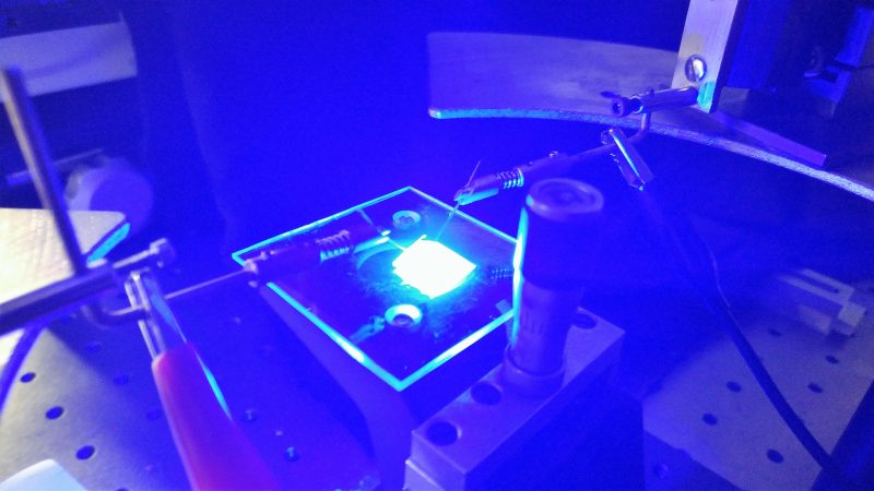
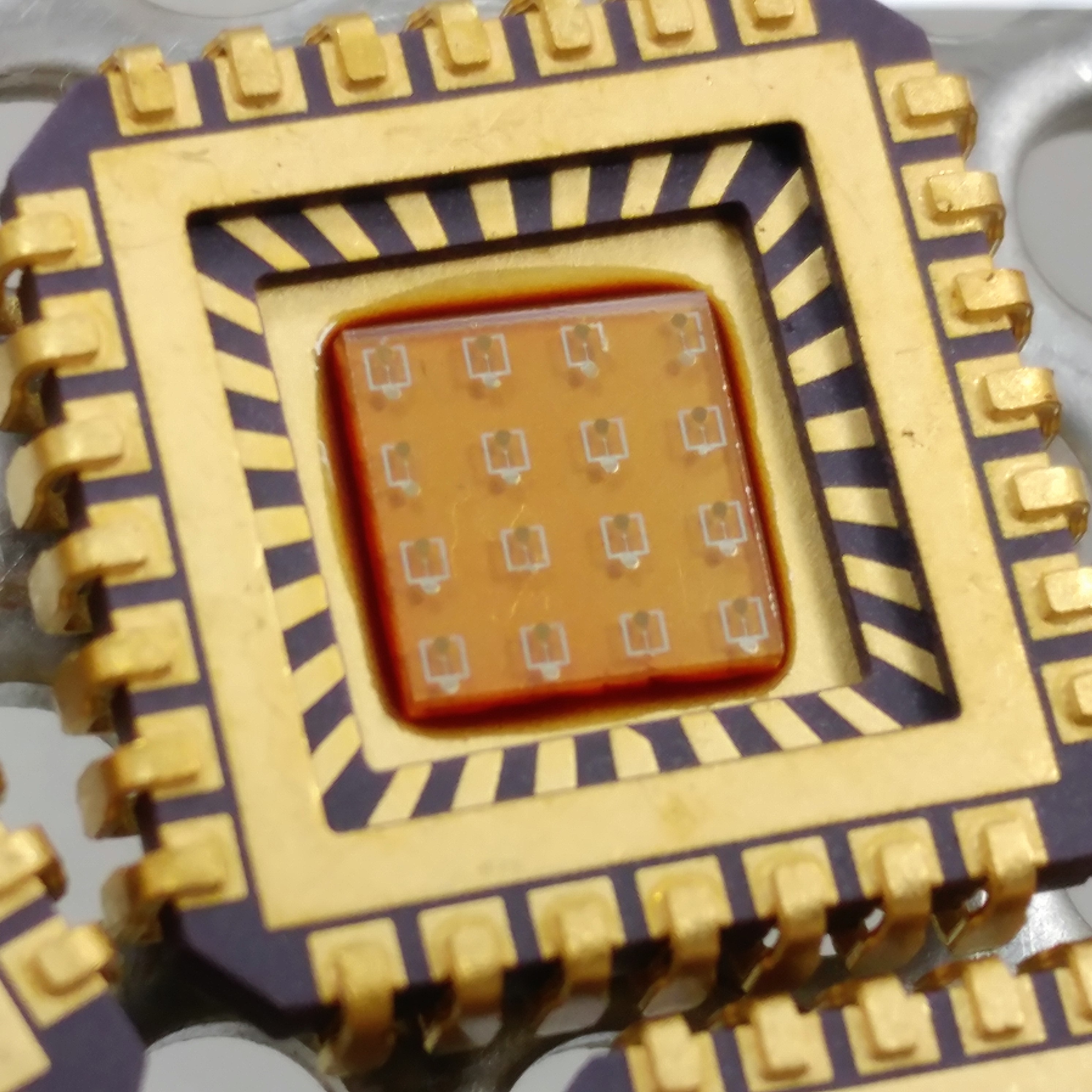 For [emach1ne], the DIY LED was part of a Master’s degree course and began with a slice of epitaxial wafer that goes through cleaning, annealing, and acid etching steps in preparation for photolithography. While gingerly handling some expensive masks, [emach1ne] got to use some really cool tools and processes — mask aligners, plasma etchers, and electron beam vapor deposition. [emach1ne] details every step that led to a nursery of baby LEDs on the wafer, each of which was tested. Working arrays were cut from the wafer and mounted in a lead frame, bonded with gold wires, and fiat lux.
The whole thing must have been a great experience in modern fab methods, and [emach1ne] should feel lucky to have access to tools like these. But if you think you can’t build your own semiconductor fab, we beg to differ.
[via r/engineering]


Back in the day (’70’s) in high school I got some Bell Labs science kits that allowed you to build your own solar cells- nasty chemicals and all…
“fiat lux”
A reference to “A Canticle for Leibowitz”?
B^)
https://en.wikipedia.org/wiki/A_Canticle_for_Leibowitz
Actually, that phrase comes from the Bible– it’s Latin for “let there be light” (Genesis 1:3). But it’s telling that people think it comes from an obscure science fiction novel. Apparently, the Bible is not taught anymore, or Latin.
Oh, I knew it came from the Vulgate, but it was the Leibowitz story that came to mind when I read the article.
B^)
Oh I see it is from a much earlier work of fiction, most interesting.
Darren,
Are you really so insecure or intimidated about the Bible that you feel compelled to discount it? Have you nothing better to do than make sophomoric attempts to insult others’ beliefs?
Christian missionaries devote their lives to discounting others’ beliefs.
Oh.. and I thought it was from here.. };¬)
https://www.youtube.com/watch?v=I9-Niv2Xh7w
I have a newfound respect for LEDs now!
LEDs revolutionized a lot of things from lighting design, to communications. But for 2018: everything nostalgic, there should be something on homemade tubes.
I can’t do you home made tubes… how about CRT repairs…
https://www.youtube.com/watch?v=byCeMKzPJgM&t=4065s
This is not “at home”, but still one dude doing it all by himself…
https://www.youtube.com/watch?v=wxL4ElboiuA
Something I don’t quite get from the process is when the P-N junction is formed. I assume the wafer is P doped on the surface and the first etch removes the P material from the unwanted zones. Is this correct?
The actual diode part was already on the wafer he started with (likely grown using some sort of vapour deposition process), all that he needed to do was isolate a device and add contacts. One if my fluorite demos working with LED wafers was touching a probe to the top of an unprocessed wafer, which causes a large area to glow dimly.
If I have access to state of the art vapor deposition chambers is there any playbook for growing the diode on polycarbonate? I work for a eyeglass lens lab, boss is open to playing around if we can produce something cool. What I’d really like is lenses with a ring of ir emitters but even if I can make lenses that glow visible when a voltage is applied boss would be thrilled. I’ve done pcb mfg before, I assume it’s going to be a more additive version of that
“If I had dropped one of these I probably would have stood up, walked out, and never returned.”
no you wouldnt you would go back to the start and etched a new one and then raised the price of the leds made from that plate by a factor of double to make up for the loss of the previous plate.
or salvaged the unbroken etchings and then only raised the price of the difference between unsalvagable etchings and the value of a perfect plate
I have an ORI UV exposure unit if anyone is interested. 500+ watts of UV, not dangerous at all. ;-)
I bet it makes great toast.
Of cause, but you toast will have melanomas all over ;-)