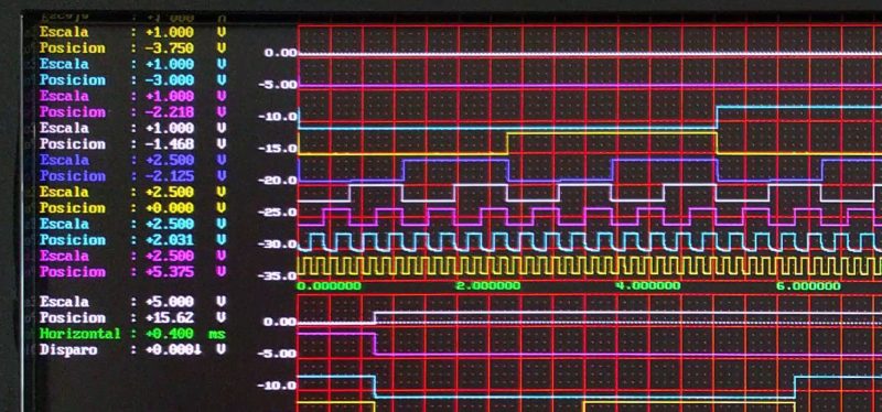
Have you ever found yourself in the need of a nine channel scope, when all you had was an FPGA evaluation board? Do not despair, [Miguel Angel] has you covered. While trying to make sense of the inner workings of a RAM controller core, he realized that he needed to capture a lot of signals in parallel and whipped up this 9-channel digital oscilloscope.
The scope is remote-controlled via a JavaScript application, and over Ethernet. Graphical output is provided as a VGA signal at full HD, so it is easy to see what is going on. Downloading sampled data to the controlling computer for analysis is in the works. [Miguel] runs his implementation on an Arty A7 development board which is currently available for around a hundred dollars, but the design is transferable to other platforms. The code and some documentation is available on GitHub and there is a demo video after the break.
Oscilloscopes occupy a special place in hacker lore, be they analog home-made ones, units used to play Quake, or being tricked into working outside their specifications. The last one even features comments that recommend the use of an FPGA similar to the one used here.


I bought the Saleae Logic Pro 16 when it was a kickstarter a few years ago. It can do mixes of 16 inputs of analog and digital, within the bandwidth of a USB 3.0 link. There are bandwidth tradeoffs depending on how many channels are used and for what. I got their old Logic 8-input digital data analyzer a few years before that, and since I liked it so much, I bought into their kickstarter. Too bad I retired since then, so I don’t come across the need for all that capability that often anymore. Check it out at saleae.com. They even have an SDK to extend and write your own stuff.
they recently released a Live Mode beta. game changer!
FPGAs are getting more capable, especially if Xilink’s project Everest works out. Biggest issue has usually been cost, with the next being documentation.
For me it’s always been programming the thing
I’ve always had trouble translating VHDL/Verilog into a configuration bit-stream for the things. Usually once that step is done, the rest is easy.
About the only one I’ve had success with is the iCE40 (thank-you Clifford Wolf).
Really? The vendor tools (Vivado, Quartus, Diamond) are all pretty straightforward to get to a config file, with more or less the same flow:
1) Create a project for the part
2) Add your Verilog files. Maybe tag one as your toplevel module if the tool can’t figure it out.
3) Preferably make a synthesis constraint file (.sdc) to tell the system how fast your clocks are. Might get dodgy synthesis without this.
4) Make a pin map. Varies by vendor how to do this, but most of them have graphical tools to do this. Just match the pin number to the name on your toplevel module.
5) Hit compile and make a snack.
You forgot some steps…
-2) Sell your first born to be given the right to download the software.
-1) Spend two days downloading a 80GB file from their website.
0) Unpack it and sacrifice a goat whilst attempting to install their 200GB bloaty piece if proprietary software.
Compared to… apt-get update && apt-get install icestorm
Use ice storm, for the ice40 fpgas from lattice.
I do :-)
It’s the only one that actually does what it says on the tin.
Agreed. I am not a great coder, but I had more issues than expected. Kinda made me wish I was younger and in college to have the benefit of working with fpgas in a classroom setting. Glad to see others more capable than myself doing some really impressive projects :)
I was expecting a digital storage scope and not a logic analyzer.. bummer
Well it’s a digital scope, it does not analyze anything
It doesn’t seem like it is actually an oscilloscope, i.e. that it would measure the voltage of the channels. Even digital oscilloscopes usually have at least 8 bits per channel measurement.
Instead this seems to be just 1-bit per channel, which is usually called “logic analyzer”, even if it does not have actual analyzer/decoder functions.
Could we say this one has a one bit flash ADC?
The Artix 7 has: ” A user configurable analog interface (XADC), incorporating dual
12-bit 1MSPS analog-to-digital converters with on-chip thermal and
supply sensors.”
It’s more than one bit. The title image clearly shows signal rounding on some of the channels.
Its not an oscilloscope
As there are other youtube videos by the same guy, on the same board, there is a video with an 800kHz sine wave input to the FPGA oscilloscope. It’s _not_ an logic analyzer.
https://www.youtube.com/watch?v=5HWeHF17MLQ
The basic idea could be extended to work as a ramp ADC with the addition of a comparator per channel. Have the FPGA to output a ramp signal as PWM, feed that signal (via an RC or other simple filter) into one input of each comparator, apply the signal to be measured to the other input of each comparator, and read the PWM output. Should be good enough for sub-MHz frequencies.
It’s a lot easier to just feed it into multiple channels and use different voltage thresholds using LVDS inputs. That gets you basically the analog bandwidth of the LVDS inputs, which is *much* better than sub-MHz frequencies (with decreased resolution).
https://www.bunniestudios.com/blog/?page_id=24
Of course, you can do *much* better than that if you just combine the ridiculous speed of FPGAs (~sub-nanosecond carry chain delays) with tons of calibration. That’ll get you 200 MSa/s and ~10s of MHz of analog bandwidth.
http://cas.tudelft.nl/fpga_tdc/ADC_basic.html
We used to call them logic scopes. There is open source analyzer code available. An HP analyzer that would display the logic states and convert specified lines into 68K or 6502 processor instructions was as much as $20,000 in the 1980’s.
Damned! I want a digiscope, any kind. My first scope was a small one with a smaller 3″ circular screen. it was “made in Germany” so pre WW2 I presume. It only went to 120 kHZ!! Second and current have been donated university ones destined to be thrown out because someone dropped them down the stairs. So flickering screen, bad focus, calibration is in the woods and changes while measuring. Pressing one button turns a random setting on. But it works to hunt ripple and detecting data and signal lines, but not much else!!!
“Have you ever found yourself in the need of a nine channel scope, when all you had was an FPGA evaluation board?”
No, I don’t believe I have ever been in that situation, or ever will…
cool, I like it – especially the remote control.
whipped up in just 3000 easy commits!
I’ve been seeing these FPGA evaluation boards come up now and then on eBay for less than the cost of the FPGA and wonder about the ability to solder new FPGA’s in their place later on also. I picked up an NI ELVIS prototyping console and notice they have FPGA prototyping boards also and was wondering the range of FPGA packages for a more universal socket and/or socket that is more universal for adapters so the prototyping board can be upgraded at a later time.
I’m guessing there isn’t a standard FPGA hardware pinout format so most likely the above idea isn’t so easy.
I wound up recently ordering a MCU123 Saleae Logic clone and a Lcsoft Mini Board to learn logic analysis with since I’m not ready for FPGA’s yet. Still, the more advanced FPGA’s evaluation boards seem impressive with more potential if using a faster system without the limiting data transfer control point of USB 2.0; like better to use Cat 5, USB 3.0 and even on board PCI slot for more real time performance potential.