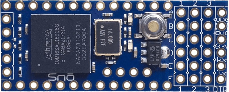
Alorium rolled out a new product late last year that caught our attention. The Sno (pronounced like “snow”) board is a tiny footprint Arduino board that you can see in the video below. By itself that isn’t that interesting, but the Sno also has an Altera/Intel Max 10 FPGA onboard. If you aren’t an FPGA user, don’t tune out yet, though, because while you can customize the FPGA in several ways, you don’t have to.
Like Alorium’s XLR8 product, the FPGA comes with preprogrammed functions and a matching Arduino API to use them. In particular, there are modules to do analog to digital conversion, servo control, operate NeoPixels, and do floating point math.
However, you can reprogram the FPGA to have other functions — known as XBs or Xcelerator Blocks — if you like. The only problem we see is that, so far, there aren’t many of them. In addition to the stock XBs, there is one that will do quadrature decoding for dealing with things like shaft encoders. There are a few others you can find on their GitHub page. You can get an idea for the workflow by looking at this tutorial for the XLR8 board.
Of course, you can write your own FPGA configurations as you see fit, but they also provide a standard workflow — OpenXLR8 — that lets you build your own blocks that operate just like their blocks. It would be easy to imagine an “app store” concept where people develop custom blocks and make them available.
We really like the idea of this device and it is certainly inexpensive. You can prototype on the XLR8 which looks like a UNO or you can put headers in the Sno. They also sell a breakout board that will make the Sno physically more like an UNO. We are surprised, though, that there are not more XBs created over the last two years.
The FPGA onboard is similar to the one on the Arrow board we looked at earlier this year, although that has some additional components like SDRAM. If you are looking for a project, it might be interesting to convert our PWM code into an XB.
Thanks to [K5STV] for showing us one of these.


Psoc-4 anyone?
No thanks.
I’ve worked quite a bit with the PSoC4 and 5LP devices. While they do have decent analog peripherals and the ability to route any signal to (almost) any pin is awesome, the programmable logic is just too little to do anything truly useful with. 8-bit data paths to the UDBs is a real head-scratcher of a decision on Cypress’ part as well, but truly, having to use that godforsaken IDE is just the final nail in the coffin as far as I’m concerned.
Now if you were to take the SiFive core, tack some good peripherals on to it and combine that into this Sno board… That may be something worth pursuing!
There are plenty of FPGAs with ARM cores in them and you can always run a RISC-V softcore in a larger fabric FPGA. Digilent’s Arty A7 can run a RISC-V processor and has a decent amount of peripherals for only $50 more.
https://forums.xilinx.com/t5/Xcell-Daily-Blog/Andrew-Black-hijacks-Digilent-s-90-Arty-Dev-Board-and-places-a/ba-p/775817
https://store.digilentinc.com/arty-a7-artix-7-fpga-development-board-for-makers-and-hobbyists/
PSoC4 are Very cheap and good. PSoC5LP are a few times more expensive, but better and great for quick prototypes: http://www.cypress.com/documentation/development-kitsboards/cy8ckit-059-psoc-5lp-prototyping-kit-onboard-programmer-and
An iCE40UltraPlus 5K seems like it would be a better fit for this sort of thing. It has 128KB of on-board SRAM which would be very nice on a small soft-core micro – in addition to 15KB of EBR. The rest of the soft-core program flash could be stored on the same config flash the programmable logic uses. Only comes in one hobby-friendly package though – QFN48. Integrated hard IP (2x I2C, 2x SPI, PWM, timers, etc) and constant current LED drivers are icing. Icestorm has basic support now as well.
The ICE40 series is OTP, not flash. You can still reprogram the SRAM but you only get to burn it in once.
That’s not completely accurate. All of the ICE40 series support external configuration flash and configuration over SPI.
Yes, that’s true. I’m only saying that they don’t have built-in flash like the Max10 or the MachXO2.
True, but a 2M SPI flash is under a dollar without trying, and the 5K configuration is about 128k so there’s plenty left over for application use.
I know it is OTP. The config flash I was referencing is external. You only need 100KB or so for the device config at the start of SPI flash. Add a bootloader ROM in EBR to pull in the rest of the soft-core app code from SPI flash beyond that into SRAM. 143KB of total SRAM (15 EBR, 128 single-port) is quite a lot for a small programmable device. MAX10 goes up to 182 KBytes (EBR) on their largest device and only 21 KBytes (EBR) on an equivalent sized device.
“Hobby friendly” packages aren’t that important here, I think most hobbyists would just use the whole breakout board.
The MAX10 is an awesome part, if you need programmable logic.
However, it’s pricey, compared to a microcontroller. The part on that board comes up at $33 on Digi-Key, qty=1.
If you’re not making extensive use of the custom logic functions, it’s an expensive way to implement an embedded controller.
Somewhat baffling is the choice of the 10M16 part when the 10M08 should have had plenty of space for the intended use and costs less than half the price.
The lower end MAX10 parts have loads of restrictions that are not immediately apparent. I’m using a 10M08SCE144C8G and you can’t use the onboard memory as a pre-programed ROM. It also lacks the ADCs and DDR memory interface.
normal linux + fpga very usefull.
where do you plug your usb cable ?
You either need the daughterboard or a USB to TTL RS232 converter. I think it is pinned out for a common one.
The text suggests it’s an AVR chip with an FPGA attached to it, but it seems to be an FPGA with an AVR compatible softcore, right?
Correct. That text comes from Alorium’s website, btw, which seems a bit disingenuous of them.
Hi BeagleBoy – which part seems misleading? We have tried very hard to be sure we are clear in the descriptions of what is on our boards. The fact that it’s still a bit confusing is good information. Any details you can share will help us clarify things better. Thanks!
The main product page says “EMBEDDED 8-bit AVR instruction set compatible microcontroller”, and then mentions FPGA-based Xcelerator Blocks, which makes it sound like there is a dedicated microcontroller and separate FPGA extensions. It is clarified on the Xcelerator Blocks page that the microcontroller itself is realized on the FPGA, but I think it’s worth mentioning it on the product page as well. It’s really no big deal though.
Wow that video is EWaste, Should’ve just done a simple page for it.
Is this thing called the Sn-not-o? Snotto. I like it.
Haha! I really think it’s “snö”. Swedish for snow.
That’s sno bull!
B^)
From the part number / data sheet – single supply, 169 pins in 11mm x 11mm UBGA package (0.8mm pitch).
16K logic elements (LE). 12-bit, 1Msps ADC
External memory: only on devices with dual power supplies (Sorry, no DDR3 SDRAM support on this chip).
DSP: 45 18×18-bit multipliers
By using the single supply chip, they don’t need to support high speed SDRAM – or any other high speed interface. That simplifies their design significantly, but is something to consider if high speed is your big reason for switching from microcontrollers to FPGAs.
Is there a software setup which allows schematic entry for fpgas? cause the idea of programming gives me the blues
Yes, the Altera tools support that. No, it really isn’t useful beyond basic work and you should take the time to learn Verilog or VHDL.
Years ago I felt like that too. But let’s try a thought experiment. I have a 4 bit number coming in and I want to drive a LED display with 0-9 based on that input. I can draw the schematic out. Might make a mistake or two but it wouldn’t take long. Decode each digit and drive the segments.
There here’s the code in Verilog:
reg [7:0] Disp;
assign {segA, segB, segC, segD, segE, segF, segG, segDP} = Disp;
always @(*)
case(BCD)
4’h0: Disp = 8’b11111100;
4’h1: Disp= 8’b01100000;
4’h2: Disp= 8’b11011010;
4’h3: Disp= 8’b11110010;
4’h4: Disp= 8’b01100110;
4’h5: Disp = 8’b10110110;
4’h6: Disp= 8’b10111110;
4’h7: Disp = 8’b11100000;
4’h8: Disp= 8’b11111110;
4’h9: Disp = 8’b11110110;
default: Disp = 8’b00000000;
endcase
That took no time at all and is easy for almost anyone to look at, understand, and correct. Now imagine doing a 32-bit CPU in schematics (I used to have access to the 68000 family schematics; they covered giant tables and were multiple sheets). Much better to describe using Verilog/VHDL/etc.
So what exactly can it do better than standard Arduino without having to leave the Arduino IDE / household programming experience?
real time signal processing/control for one. You can create the VHDL/Verilog for the heavy lifting of some DSP algorithms then write super sloppy code to deal with the results.
Does it have some predefined high level functions or do I have to write VHDL?
Yes. There are a few pre defined functions available. All mentioned in the article. All are available in the arduino ide. You simply choose the block you want to use and burn that bootloader. Once configured you upload your code just like any other sketch with the exception of using the custom libraries instead of the standard ones.