
Last time we looked at Spice models of a current sink. We didn’t look at some of the problems involved with a simple sink, and for many practical applications, they are perfectly adequate. However, you’ll often see more devices used to improve the characteristics of the current sink or source. In particular, a common design is a current mirror which copies a current from one device to another. Usually, the device that sets the current is in a configuration that makes it very stable while the other device handles the load current.
For example, some transistor parameters vary based on the output voltage which causes small nonlinearities in the output. But if the setting transistor has a fixed voltage across it, that won’t be a problem. The only problem with mirror schemes is that the transistors involved all have to match in key characteristics. For that reason, mirrors are usually better on ICs where the transistors are all more or less the same. You can get discrete transistors that have multiple devices built on a single substrate, but these are not very common.
Note that the operative words are “key characteristics.” Some parameters can be different. For example, on an IC with MOSFETs, it isn’t uncommon to use one transistor to set several currents. The output transistors will have different channel widths and that will scale the reference current up or down.
Motivation
There are lots of places where it is handy to have a current source or sink. We’ve looked at LED drivers, of course. Battery charging and electroplating often require — or at least desire — a constant current. One of the most common uses, however, is to use them as bias elements for high-precision amplifiers.
When you bias a transistor with a resistor, you are really assuming you understand how much voltage will be across the resistor and, thus, set the current. However, in real life circuit parameters may vary both between circuits and even over time. Changes in voltages across bias resistors change currents, and that shifts the bias.
If you look at the schematic of what’s inside a typical op amp, for example, you’ll see current sources and sinks are used on nearly all the amplifying transistors. We’ll save the details of that topic for another installment, but be aware that there are many uses for these current sources and sinks.
Transistors
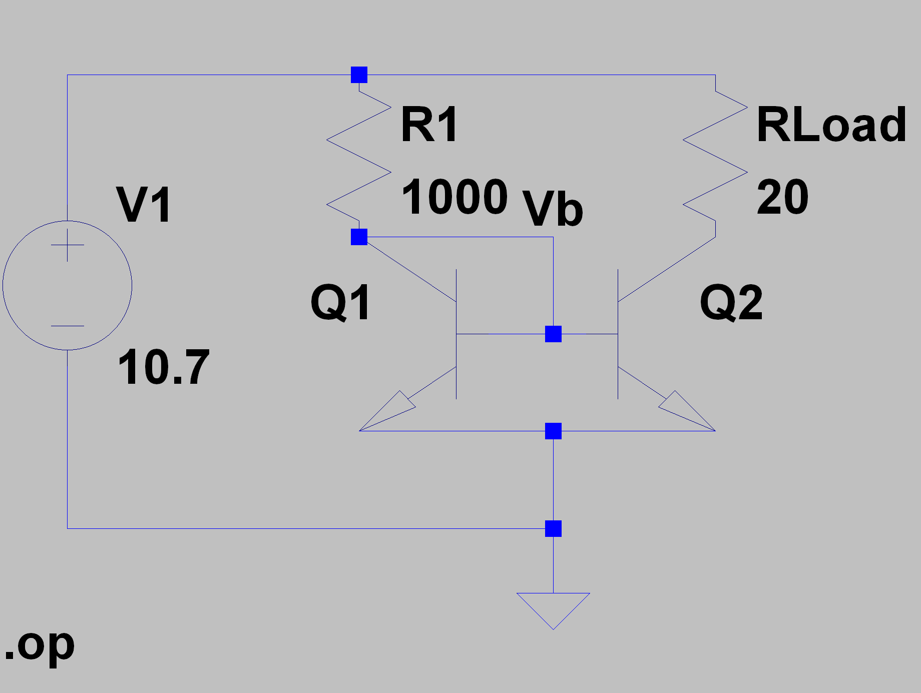 Let’s look at a transistor mirror. This mirror works best when the two transistors are matched. That is, they have the same beta and will have the same Vbe drop. The better they are matched — including how they react to things like temperature or changes in voltage — the more accurate the current mirroring will be.
Let’s start with the left-hand side. We know the base of Q1 will be at about 0.7 V or so, because the emitter is at 0 V. Since Q1’s collector is tied to the base, the voltage across R1 will be the supply voltage less 0.7 V. I cheated and made the supply voltage 10.7 V to make the math easy. That means the current through R1 — the Q1 collector current for all practical purposes — must be 10 V / R1. For that to be true, the base current has to be roughly that same current divided by the transistor beta.
Because the transistors are exactly the same, whatever current is passing through Q1’s base must also be flowing through Q2’s base. And the Q2 collector current must be the base current times beta, which is matched to Q1’s beta. With the same base current and the same betas, the current passed through Q2 must be the same exact current we started with — the current through R1.
There are two problems that arise with this circuit in real life. First, I’m ignoring some small currents so the numbers will be a little off. As long as the beta of the transistors is high, the error will be very small. The second problem is the beta. Transistor beta varies within a pretty wide range even for the same type of device. We usually design so that those variations don’t matter. In this case, we don’t really care what the beta is exactly, but we do care that they are the same. If they aren’t, the results will be off. You can get dual transistors in one case where the device is on one piece of silicon. For example, the SSM2212 has two transistors. Their beta values are matched to within 0.5%.
LTSpice
If you try the LTSpice simulation (see GitHub if you don’t want to draw it yourself) you’ll see that the numbers prove out. Here’s a sample run:
--- Operating Point ---

V(n001): 10.7 voltage
V(vb): 0.7177 voltage
V(p001): 10.4845 voltage
Ic(Q2): 0.0107746 device_current
Ib(Q2): 5.06865e-005 device_current
Ie(Q2): -0.0108253 device_current
Ic(Q1): 0.00988058 device_current
Ib(Q1): 5.10312e-005 device_current
Ie(Q1): -0.00993161 device_current
I(Rload): 0.0107746 device_current
I(R1): 0.0099823 device_current
I(V1): -0.0207569 device_current
Note the base voltage is just over 0.7 V. The current through R1 is just under 10 mA and the current through the load is just over 10 mA. Of course, you can require more voltage than is possible. Try changing the load to 20 kΩ instead of 20 Ω. You can also change the transistor parameters to evaluate the effect of having unmatched devices.
Wilson
 The current through Q1 and Q2 are slightly different. That is known as a static error. The static error, in this case, is actually pretty large as a percentage with the load seeing 10.8 mA from a programming current of 10.0 mA, rounding to the nearest tenth. Clearly, that’s an 8% error: 0.8 divided by 10 then multiplied by 100 to make it a percentage.
In general, a mirror is “better” if the percentage of the static error is lower. In other words, 1 mA out of 2 is terrible, but 1 mA out of 2 A is not so bad. In this case, 800 μA doesn’t sound bad, but it is 8% of the total.
In fact, there are three things that define a better current mirror:
- Minimize static error
- Maximize output resistance (or, inversely, minimize conductance)
- Minimize the minimum operating voltage
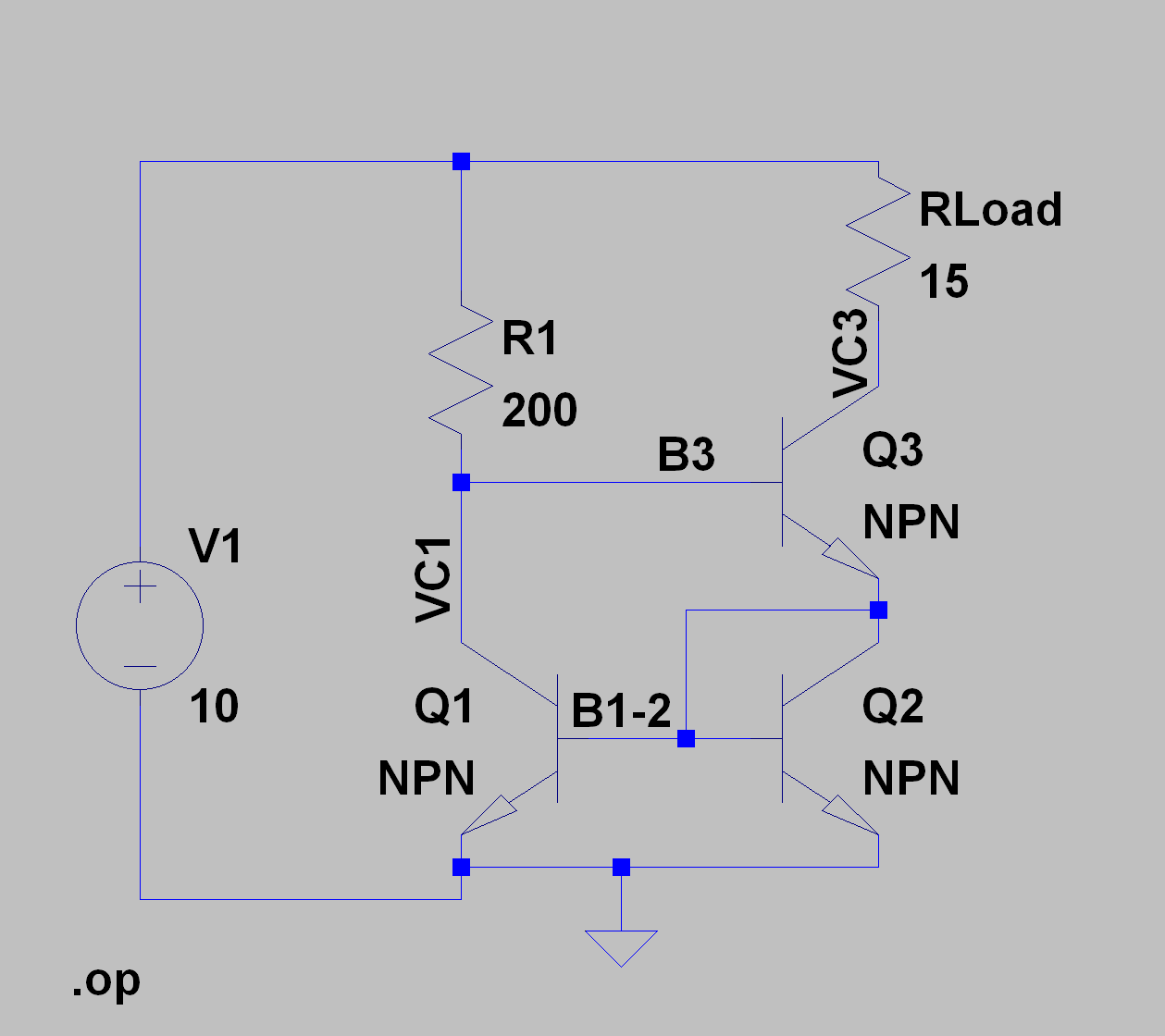
There are several other architectures that attempt to address these problems. One of the most common is the Wilson current mirror. It uses three transistors as you can see in the schematic.
Before we look at how it works, let’s see if it does work. Here’s the output of a simulation:
--- Operating Point ---

V(vc1):  1.74067  voltage
V(b1-2):  0.870209  voltage
V(vc3):  9.38067  voltage
V(n001):  10  voltage
Ic(Q3):  0.0412888  device_current
Ib(Q3):  0.000412888  device_current
Ie(Q3):  -0.0417016  device_current
Ic(Q2):  0.0408839  device_current
Ib(Q2):  0.000408839  device_current
Ie(Q2):  -0.0412928  device_current
Ic(Q1):  0.0408839  device_current
Ib(Q1):  0.000408839  device_current
Ie(Q1):  -0.0412928  device_current
I(R1):  0.0412966  device_current
I(Rload):  0.0412885  device_current
I(V1):  -0.0825852  device_current
Here, the set current in Ie(Q1) is 41.3 mA. The output current through Rload is also 41.3 mA (again, rounding to the nearest tenth which is 100 microamps). If you trust the significant digits, the output is off by about 4.3 microamps. Now the error is about 0.01%. In reality, you won’t make this number for a couple of reasons. The transistors must be perfectly matched, for one thing. A variety of other factors like noise and thermal gradients could affect things, too, and that won’t show up in this simple simulation. Still, even if it is off by a factor of 100, it will be about 1% off which is a lot better than the 8% we had before.
How Does That Work?
You wouldn’t think that adding more parts would make the circuit more accurate. The trick is, though, that the transistors match. As current comes into the collector of Q1 it also enters the base of Q3. Assuming there’s enough voltage to forward bias Q3, it acts like an emitter follower. Voltage rising on the base causes a corresponding increase on the emitter (reduced by a diode drop).
That voltage feeds the bases of Q1 and Q2. The net effect is that everything rises until Q1’s collector current plus Q3’s base current exactly matches the input current. At that point — remember all the beta values should equal — the base currents are all nearly equal and you get the great matching that you see in simulation. If some parameter is perturbed, the system will correct itself as long as the transistors stay matched.
If you experiment a bit with changing R1 and the input voltage, you’ll see how all the items change to stay in sync.
So the Wilson mirror is better, right? Well, as with anything there is no free lunch. Yes, the static error goes down. But the component count goes up and additional noise and frequency-dependent effects occur. Furthermore, the Wilson mirror requires more voltage than an equivalent circuit.
There are other architectures with different tradeoffs including a Wilson circuit with four transistors instead of three. Other circuits with names like Widlar and cascode have different plusses and minuses.
Analog circuit design is somewhat like chess. You can learn how pieces move pretty easily. But mastering strategy takes a lifetime. Current mirrors are just one more trick in the transistor magic hat. The real trick is applying them and combining them with other elements to get desired behavior.


I have used them to move an analog signal from ground reference to + rail reference and vs versa. Wilson current mirror rules.
“Try changing the load to 20 kΩ instead of 20 kΩ.” and “Furthermore, the Wilson mirror requires more voltage than an equivalent circuit.”
I had already caught the 20k… not sure if I did that or if was when they added the typography, but either way. Not sure what you are saying about the 2nd point, though. To meet the same compliance range, you have to have a higher voltage into a wison mirror than the vanilla circuit because there’s more drop involved.
“not sure if I did that or if was when they added the typography,”
So….
What you’re saying is, “they” (the Evil Overlords) actually insert typos into Blog texts…
Hmmmm….
Nah, we have great editing, but either way, fixed ;-)
Me. He meant me. Dangit!
I think you meant “requires more voltage than the simpler two transistor circuit.”
The other big advantage to having both devices on a single die is that they’ll be at the same temperature. Discrete devices can be at different temps, causing one Vbe to exceed the other, and unbalancing the current. In extreme cases, this unbalance causes one device to heat even more, causing more imbalance, and so on, leading to thermal runaway. This isn’t really surprising, since you essentially have connected two base-emitter diode junctions in parallel, and we know the perils of parallel diodes.
Question: how do you modify the basic two-transistor version to multiply the current by a controllable factor?
I don’t want to spend 10 milliamps in vain to get 10 mA at the output.
Put a resistor under the emitter of the diode-connected reference transistor. That’s the Widlar current mirror.
Current mirrors take advantage of the relationship between Vbe and Ic: increasing Vbe by about 60mV increases Ic by a factor of 10. The diode-connected transistor finds the Vbe necessary to allow a given amount of Ic through the collector. Connecting that voltage to the base of a matched transistor gives that one the same Vbe, so the Ic will also be the same.
If you add an offset voltage to the diode connected Vbe, it works as a multiplier for the output transistor’s Ic. If you send 100uA through the diode-connected transistor you get a usable Vbe, then add 120mV to that voltage, the output transistor’s Ic will be about 100x larger. At 100uA and 120mV, you’d want a 1.2k resistor.
Widlar used the idea the other way around, putting the resistor under the output transistor to get nanoamp output currents from mid-microamp reference currents. The principle works either way though.
So the base currents divide by the difference in voltage offset.
I found the same solution through experiment, but I’m having trouble adapting it properly. You see, I’m trying to make an envelope generator with an adjustable rise/fall time between about 10 ms to a couple seconds without straining the uC output or wasting current, and I’m trying to be clever without adding yet another op-amp to the circuit. Also, the output must go very close to ground, but not necessarily to Vcc – to save on adding offset trimming.
The circuit so far:
http://tinyurl.com/yd2vzx9q
Oh, mind that the potentiometers in the simulator operate with 1:200 steps i.e. the smallest value is 5 Ohms with the largest being 995 Ohm. It’s that last little nudge that makes a huge difference and makes the circuit very fiddly.
It’s a tall order to ask for a range of 200,000x. I need it to work logarithmically somehow.
Nevermind, I made a slight error. It’s 200x, not 200,000x
Anyways. I think I found the solution. Instead of adjusting the offset voltages, I’m adjusting the ratio of base currents. This seems to work and gives a nicely adjustable rise/fall time so the linear potentiometers have a logarithmic effect:
http://tinyurl.com/yc58gzua
Only question now is how to put this into an equation so I can see what really happens.
If in the basic diode configuration, I add resistance to the base, does that simpy do the same thing? Make it effectively seem like a diode with a higher treshold voltage?
Temperature cooficients of the diodes generate big errors here if there is a temperature difference between the diodes, Putting them on the same die would be ideal.
Connecting 2 TO-92 packages together with the flat sides and wrapping a piece of copper wire around them also helps to keep them on the same temperature, but most of the heat conduction would be through the legs, not the package.
For more practical circuits, build the current mirror with 2 resistors, an opamp (to compare voltages over those resistors) and a MOSfet on the output of the opamp.
This has:
– better accuracy.
– Much less temperature dependency.
– About the same number of components (you may even have a spare opamp of a 4 opamp chip)
– Easy to adjust current ratio’s by using different values for the 2 resistors.
You can also buy this in pre-packaged format. High-side current monitors are often build around this principle.
Difference is that the shunt resistor is put between the resistors to the opamp and becomes therefore a part of the measurement circuit.
Why the copper wire, just use some heatshrink tubing.
Thanks for the article, Al! Keep the analog articles coming!
I love this series. It’s as if someone is considerately taking me through The Art of Electronics, which I’d have little confidence to just dive into.