There was a time when reflow soldering was an impossibly exotic process at our level, something that only the most superhuman of hackers could even dream of attempting. But a demystification of the process plus the ready availability of affordable PCB and stencil manufacture has rendered into the range of almost all constructors, and it is likely that many of you reading this will have done it yourself.
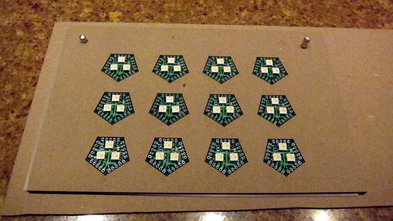
Screen-printing solder paste onto a single board presents a mild alignment challenge, but how about doing it with many boards at once? [Eric Gunnerson] had this problem with a small-volume board he’s selling, and not being in the happy position of having his PCBs supplied on a panel, had to create his own multi-board alignment jig and stencil. His write-up provides a comprehensive and fascinating introduction to the process whether you are an occasional dabbler or embarking on a production run as he is.
The problem facing any would-be stenciler is that the board has to be held in place reliably in the same alignment as the stencil. With a single board, it’s easy enough to do the usual thing of taping scraps of PCB board to constrain its edges and hold it in place as a rudimentary jig, then lower the stencil onto it. Perhaps you’ve used one of those commercial stencil jigs, in which a set of magnets hold the stencil in place, or maybe you use pins to line everything up.
[Eric] takes us through the process of creating a laser-cut alignment jig for twelve boards, and cutting a matching twelve-board stencil. This includes all the software side using Inkscape, the selection of materials to match PCB thickness, and some of the issues with cutting Mylar sheet for the stencil without shrinkage at the corners. He’s using pins for alignment, and he even finds a handy supply of those in the form of shelf support pins.
We’ve visited the world of reflowing many times before. If you’d like a primer, here’s our Tools of the Trade piece on it, and if you aren’t daunted by larger projects, here’s an account of a prototype run of a significantly complex board.


Just a note for others. It looks like he ordered 120 boards without thinking of putting them on a panel… that’s fine, just about everyone does that at first.
However… “not being in the happy position of having his PCBs supplied on a panel”… ? That’s something YOU do, not them. (almost always, anyway) Once you notice the problem… take the time to organize your board into panels and order that way. For his design, he might even save some money doing a better job of packing them than a board house might normally bother with.
He seems resourceful, he probably doesn’t need me telling him that. It’s worth saying, though.
I’ve had many moments like this that alter how I design things… here are just a few off the top of my head. Many are pretty obvious, but I still usually had to do things once the hard way before adjusting:
1) A stencil printer (manual, at first), a pick and place machine, and a reflow oven nudged me to optimize the following:
a) Panels, to do many more boards at once. You’ll need at least 0.2″ rails on the top and bottom, too. I’ve gone to 0.25″ over time. V-scoring seems easier/neater to me than tabs. Don’t put fiducials on the rails unless you know the pick and place grips won’t just cover them up. (Oops) Don’t go crazy though… 12” on a side is the limit that I can reasonably use with my binocular microscope setup for inspection/touch ups.
b) Moving away from components on both sides of the board whenever possible to save a lot of time.
c) Work to limit the number of distinct components you use. (Ie: Don’t have 0402, 0603, 0805, and 1206 sizes of 10K resistors unless actually required for some reason) Maybe use two 10K resistors instead of that single 20K you only use once. All those different parts you picked up from a lot of different reference designs need to be combined when possible. I had five different diodes with similar specs that got optimized to one.
d) Move to parts that are easier to assemble. SMT over through hole is obvious… but also make sure the parts are easy for your machines to actually do (in my case, I had tried to standardize on 0402 sizes of a lot of passives and this created a lot of headaches in much higher numbers of assembly touch-ups with my older equipment) Rectangular crystals instead of cylindrical, etc.
e) If you do have to have two sided loads, make sure at least one side has components all light enough for surface tension to hold them in place when you run the opposite site through later. Avoids needing glue. You’d also be surprised how large a component can be and still do that.
2) Moving from a manual stencil printer to an automatic one:
a) Stencil fiducials. I tried to order these when I bought the printer… before using it… and blew $1000 in stencils I never used. I failed to understand how the printer needed to use them (my printer expects stencil and PCB fiducials to be in the same places… I thought it would just measure them separately)
b) My stencil printer (DEK Horizons 03i) does not really move the stencil a lot in XY for adjustments. I align the front side of the panel edges at a common distance from the front of the stencil, which means with my fixed front rail on the stencil printer I don’t have to adjust the positioning of the stencil frame for different stencils. Just load and go.
c) Find good paste that has a long working life. I like LOCTITE GC 10 SAC305 no-clean solder paste.
3) Recently adding a selective solder machine (solder fountain style) has now got me going back through designs again moving SMT components further away from through hole leads, to allow for faster processing of boards once again.
Almost every time I pull some part of the manufacturing in house, I learn better ways to design for easier manufacturing. It’s a really neat process to go through.
I still haven’t even really done much work on simplifying testing. I’ve designed several boards for pogo-pin test/programming contacts, but I have yet to actually use that. There’s a lot to do there as well.
You just wrote an excellent hack a day article. Thanks!
There is a lot of good advice here, and that is said from someone who has worked in this industry for 23 years now.
I have started recently using pogo pins for the programming of and testing of the boards, and it works brilliantly for me. I designed a universal test board with all the standard interfaces I need (USB UART, Power, JTAG, etc..), and a protoboard area with 0.9mm holes in which I solder the pogo pins in positions specific to each type of board I need testing. Over that, I 3D print a cradle (socket) specific to the outline of the board to test, that will hold the board in place so that the pogo pins match the pads on the board. So far the system has worked really well, and I have managed to program and test quite a few different models of boards I have designed.
One improvement I want to do though, is to change the pogo pins for ones with a smaller terminal so that I can put them into the PCB with sockets, as soldering them can cause the springs to deform if overheated.
I’d love to get pogo-pin test fixtures going. I just haven’t quite bothered yet for the simple reason that it won’t save all that much time in my case. Most boards that get programmed are also calibrated, which takes about two minutes per board. I don’t think I’d really save much more than 3-4 seconds per board with a pogo-pin test fixture vs. four fairly simple cables. Another board has two 2×7 headers, also pretty quick to do considering the ~45 seconds it takes to program that one.
I just delivered 3x homebuilt test fixtures to our factory in shenzen. I initially estimated it to a 1 week job, but ended up taking more then 3x that time. But i got to use my 3d printer and cnc-mill and got to poke around a bit with KiCAD and FreeCAD. Now we will see if they survive the batch of 16 000 boards.. otherwise it will be easy/quick to make replacement fixtures. PCB will change for next batch anyway.
Hey Darron,
That’s a great list of things to consider. I probably didn’t make it clear in my writeup…
It’s not that I don’t know how to panelize a design. The problem is that the boards are pentagons, and because of that, there is no way to panelize them into a rectangular array. That means I can’t use v-grooves. I considered using breakaway tabs, but once again, because there is no easy way to lay them out so that you could break the boards apart, that didn’t make sense. It was just easier to let the PCB house do the panelization and then give me nice, smooth, router-cut boards. That also helps make the assembly easy.
Well, the board house has to panelize them in any case. It might as well be you. You’re right, them doing it is the only way you’d get perfect edges. However, its a lot more work that way. You can get away with only two edges having mouse bites from tabs… let me try to figure out how to attach an image.
Well, that’s a lot more work that way. You can panelize in a way to only have mouse bites on two edges. V-score one edge, route out diamonds between adjacent boards, and tabs on the remaining two sides: http://www.griffin.net/PentagonFill.png If the board house can do V-score lines on inside shapes, you could even have zero mouse bites. Just route maybe 5mm on each end of a tab line and V-score in between.
So, uh, what IS the syntax for comments here? I searched around and found nothing.
Hey Darron,
Good tips…
The boards are pentagonal, so you can’t panelize in the usual ways, and I needed a nice smooth edge anyway. So letting the board house rout them out made much more sense.
Rather than going exotic and using a laser cutter, wouldn’t be easier to panelize the boards so that they match the stencil. That is a pretty easy task and it is faster to handle one panel, rather than handle single circuits. My biggest concern is how to get the PCBs out of those slots without disturbing the components to put them in the reflow oven; they seem quite tight fit.
seems overkill for a few plcc 4’s and 2 lead 603’s, yea I understand there’s a pile of boards to do but if it were I, I would have just sucked it up and got a 1 up stencil …. actually I would have just squirted paste on the pad’s … I recently did 80 pieces with plcc 4’s at a similar component count, its not so bad if you take a break for your hand, had them done in an afternoon with no stencil
Here is my experience:
1. Do not use NXP components unless you can live with 48 weeks lead time
2. Make sure you check component availability, its a good move to spend slightly more (or less) on components you can actually get when you need them.
3. Fall back plan, check if you can support multiple suppliers with the same footprint. In our case we used an fixed voltage LDO with pin 3 as NC, two other manufacturers had a simular spec LDO but with EN at pin 3. By connecting pin 1 vcc with pin 3 NC/EN on the PCB we can select between atleast 3 manufacturers and select what is cheapest or available at the time of production.