
In the last installment of Circuit VR, we walked around a simplified buck converter. The main simplification was using a constant PWM signal. The result is that the output voltage is a fixed fraction of the input voltage. For a regulator, the pulse width will need to depend on the output voltage so that any changes in the output are self-correcting. So this time, we’ll make a regulator, although we’ll still use a few Spice elements you’d have to replace in a practical design. In particular, we’ll assume you can generate a triangle wave, which is easy enough, and produce a stable 2.5 V reference.
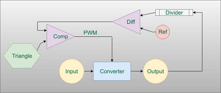
The idea is to take a voltage reference and compare it to the output. We’ll think of the difference between the two as an error voltage, and use a comparator combined with a triangle wave generator to produce a PWM signal that is proportional to the error, and thus works to hold the output voltage constant.
Playing the Triangle
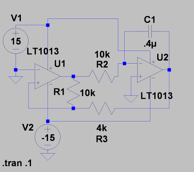
If you need a refresher on how the triangle wave and a comparator generate PWM, check back in the last post. As a refresher, here’s the architecture I settled on.
Once again, I took a junkbox approach — you could probably select better components if you had specific goals in mind and thought about it. I just grabbed likely parts and wanted to make them work, just as I do sifting through my physical junk box.
The only thing I took the easy way out on was the triangle wave generator. If you look for a specific triangle wave generator in Spice, you’ll be disappointed. But the PULSE block can do it. I set the parameters to the following:
V2 N006 0 PULSE(15 0 0 .0000005 .0000005 0 .000001)
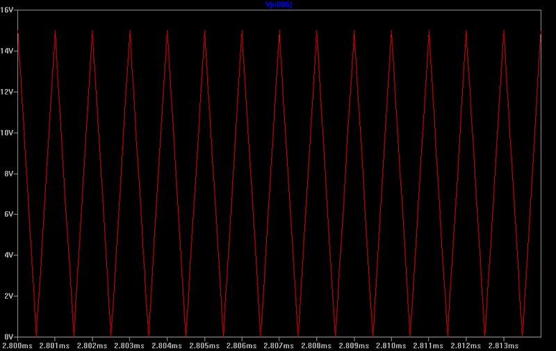 Of course, you’ll want to use the LTSpice GUI to enter that. The VInitial is 15 V, The rise time is 500 nS and the fall time is also 500 nS. The period is 1 uS. Think about that for a second. Since the rise time is half the period and the fall time is the other half of the period, the result is always rising and falling.
Inside the Circuit
You can find the files on GitHub, as usual.
I started the supply voltage (V1) at 15 V. M1, D1, L1, C1, and RL are essentially the same as the basic buck circuit seen last time. The difference is that R2 and R3 form a voltage divider that splits the voltage in half and sends it to U2. U2 is a differential amplifier comparing the voltage to V3 which is a 2.5 V reference. In a real circuit, you should make that reference voltage a good one, since the accuracy of the supply won’t be any better than the reference.
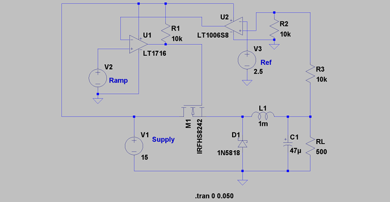 Obviously, you don’t have to have a 2.5 V reference. You can set the voltage divider ratio to convert any higher voltage to any lower reference you happen to have. The output of V2 is the triangle wave and U1 is a comparator that produces the PWM drive signal (R1 is just a pull up and, depending on U1, may not be necessary).
I’m cheating a little because I’m not driving the gate with a higher voltage which may cost me some efficiency. In a real system, you’d probably want a bypass capacitor near M1’s input side as well, to reduce noise going back into the power supply which isn’t a big concern here. I also didn’t show any series resistance for V1, V2, or V3, although if you add a little you’ll see it doesn’t really make any difference.
Performance
If you run the simulation and probe the junction of L1 and RL you’ll see about 5V come out eventually with some ripple.
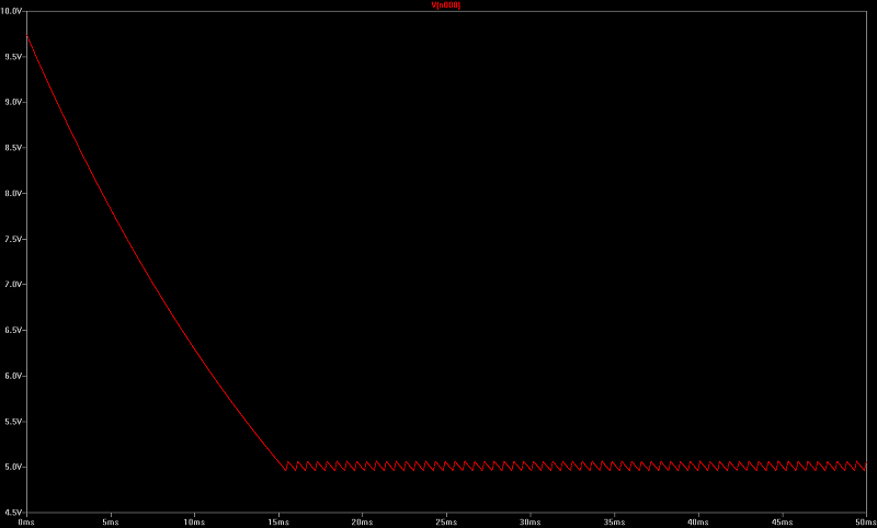
The ripple isn’t bad at all and the voltage is steady after about 15 ms.
I changed the input voltage to step between three values, and to quit plotting the first bit — before 25 ms — so we can focus on the operating area.
The output looks very ripply until you look at the left-hand scale.
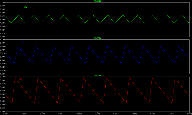
The top trace is with the 10 V input, the middle trace is for the 15 V input, and the bottom trace shows the 20 V input. Not too bad for a handful of components. Sure, you could get better with a linear pass regulator, but those dissipate a lot of heat and usually have a fairly narrow input voltage range.
Keep in mind, too, that there are more sophisticated architectures that can optimize for different criteria like minimizing ripple or achieving maximum efficiency. This circuit is about as simple as you can get and offers a good starting point for digging into other kinds of switching power supplies.
Real Triangles
The one place I didn’t provide a detailed design was for the triangle or ramp generator. The reason is — as I mentioned in the first post — in real life, you probably shouldn’t be doing all this anyway. Just buy a switch mode power supply controller from your favorite vendor and copy the design from their data sheet. You’ll spend hours building a circuit as complex as the one you can get for a buck or two in an IC package. Still, you might like to understand what is happening inside that controller even if you don’t have to build it.
If you did want to generate a triangle wave, there are many ways to do it. A constant current source will produce a nice straight line when charging a capacitor. A constant current sink can discharge the capacitor in a straight line, too. Usually, a circuit like that will have a flip-flop to pick between the source and the sink.
The other way to do it is to integrate a square wave. If you think of an integral as the area under a curve, that makes sense. The area gets bigger until the square wave goes negative. Then the area reduces at the same rate until the square wave goes positive again. Here’s an online simulation of the circuit.
If you probe the output of U1 you’ll see a nice square wave. The output of U2 will be the integral of that square wave.
Going Forward
If you are feeling brave, you might try to replace the ramp generator with a variation on the triangle wave circuit. There are many other changes you might try, such as replacing the diode with another FET that you drive out of phase with the first FET.
It wasn’t long ago [Julian] posted a video about the efficiency difference between a silicon diode, a Schottky diode, and a FET. Might be interesting to see how simulation agrees with his real-world results.
In the end, though, there are two things to remember. First, simulations are great, but the real world is going to be different. Real input sources aren’t perfect. All components exhibit behavior you wish they didn’t. Some of that you can model (ESR in the output capacitor, for example) but you can’t get it all.
The other thing to remember is that this is really to help understand what’s happening. Sure, you can build an opamp out of a handful of transistors, but why? Just buy an opamp. Same thing here. I’m not suggesting your roll your own buck converter for a commercial design. Just go buy a controller — there are plenty around. But having an understanding of what’s going on will help you make better design choices and should help, too, if you have trouble getting one of those controllers to work the way that you want.


Needs a compensator! that would be the logical next step.
i built a buck regulator using a 555 as my frequency source, an opamp in comparator mode to check the output against a zener reference, both got fed into a discrete and gate and the output of that went into my switching transistor. regulator held the voltage up to 500ma. was pretty good for something built out of junk and spare parts.
What did your gate waveform look like? One issue with this kind of setup is that a load with a noisy current characteristic (anything digital for example) will create voltage noise at the point you’re taking feedback from, which will rapidly toggle your MOSFET on and off, because you’re just passing two signals combinatorially through an AND gate. You can end up with quite high switching losses, and a rather warm MOSFET.
It’s a very elegant solution with low part count though :)
If you’re willing to write a bit of code, an ATTiny plus a MOSFET can implement an excellent buck, and you still have most of the CPU cycles left over for other tasks!
I don’t use a sim for analogue so I must be missing something.
I can’t see how this could possibly work in the real world. Perhaps you can set the op-amp gain in a sim?
Both op-amps are shown as having open loop gain so the whole circuits would just be switching on and off a square wave of the frequency of the triangle wave.
U1 “should” be open loop but the negative input should be a DC voltage proportional to the output (even if inverted in some designes). But in this case the negative input to U1 will be swinging from rail to rail (as close as the op-amp gets) because U2 has open loop gain.
And 1MHz is much higher than I have seen for any switching regulator.
Strictly speaking, comparing a triangle wave to a voltage reference doesn’t give you PWM although it’s very close in concept.
In true PWM the “ON” trigger (or “OFF” if inverted) will occur at a precise and non-varying frequency, phase and period while the “OFF” trigger will vary.
With a triangle reference both the “ON” and “OFF” trigger vary in phase compared to the triangle source.
“Strictly speaking, comparing a triangle wave to a voltage reference doesn’t give you PWM although it’s very close in concept”
How so? PWM hardware is just a counter running through either a triangle or sawtooth wave, and a digital comparator.
Maybe you are referring to the higher modulation depth due to the triangle not being rail-rail, due to op amp limitations? I am curious about this statement, but having seen your other comments I’m certain there is something of substance to it.
By definition Pulse Width Modulation varies the width of a repeating pulse.
In the case of 8-bit digital PWM when the pulse is on for 64 cycles then it will be off for 192 cycles and if it’s on for 192 cycles then it is off for 64 cycles so the total is always 256.
This is derived from a clock that is 256 times the repeating rate of the pulse. Lets say the clock is 256kHz then the repeating rate would effectively be 1kHz.
Now if we compare the phase of the PWM to the phase of the 1kHz clock then we get the following phase positions for the above example –
The pulse always starts a 0 degrees.
For a PWM value of 64 it ceases at 90 degrees.
For a PWM value of 128 it ceases at 180 degrees.
For a PWM value of 192 it ceases at 270 degrees.
Now in the case of a triangle reference comparison we get these phase angles –
For a PWM value of 64 the pulse starts at 135 degrees and ceases at 225 degrees.
For a PWM value of 128 the pulse starts at 90 degrees and ceases at 270 degrees.
For a PWM value of 192 the pulse starts at 45 degrees and ceases at 315 degrees.
So a triangle reference changes phase as well as pulse width and as such is not strictly PWM.
In most cases both methods are effectively the same. However in some cases this may need more consideration.
In cases where the PWM (or Pulse Phase Modulation) is used with something like a CR low pass filter there is no real difference.
Also when your using the PWM (or Pulse Phase Modulation) for a responsive load with negligible parasitic capacitance or saturation like a LED then there no real difference.
However there can bee issues with driving an output stage like a bipolar transistor that has a higher saturation characteristic or with parasitic capacitance when you get to very low, or very high values of PWM.
At an 8-bit PWM value of 128 (50% duty cycle) the fundamental is the same as the 1kHz example above.
At any other value you have two fundamental frequencies. The lower fundamental is never more than half the clock ie 0.5kHz (500Hz) in this example but the higher fundamental will get to 256 times the clock ie 256kHz for the PWM values 1 and 254 and these higher frequencies can play havoc with saturation and parasitic capacitance and leave you with a smoldering FET or BJT.
So in the case of switching something like a BJT or even a FET you would probably want to restrict the variation range to 75% or 50% of the full range ie PWM values between 32 and 224, or PWM values of between .64 and 192 respectively.
This is why you often see a load resistor built into the output of switching regulators. If the load resistor is 100mA and the rated output is 1A then you have a range factor of 10. If the load is 100mA and the output rating is 10A then you have a range factor of 100. But! if you have no load then the range factor is extremely high.
This makes a triangle reference a little easier to use for switching regulators.
OnSemi’s TL431 datasheet has a simple buck converter circuit that doesn’t require any comparators or op-amps.
https://www.onsemi.com/pub/Collateral/TL431-D.PDF
What’s a good online sim for analogue circuits like this has good schematics?
I tried one that has good schematics but if you don’t quite draw the lines correctly then you end up with teravolts – perhaps I should make my own hadron collider with and op amp to drive it.
I tried another but it used op-amp IC pictures instead of the correct schematic symbol.
I can’t really recommend an online simulator (I used one in the past, but it has since become a paid service. Also, it wasn’t that great at the time).
I moved to LTSpice fairly quickly and haven’t looked back. It’s not as intuitive, and the learning curve is a bit different, but it’s easy enough to get simple stuff working. It’s one of those programs which are very powerful in their simplicity. Rather than having a few, pre-defined specific functions, it is quite low level, which allows to build anything you might want. Being able to perform parameter sweeps is very useful.
I only ever use a very limited sub-set of its functions. Typically idealized components, such as resistors, capacitors and ideal op-amps, together with voltage or current sources. Then I check myself if e.g. the op-amp is operating outside its design range for the given type and application (e.g. negative output voltage is not possible if the design is for a single supply). Downloading and installing model definitions is too much hassle for me considering how infrequently I do this.