Sometimes I wish FETs had become practical before bipolar transistors. A FET is a lot more like a tube and amplifies voltages. Bipolar transistors amplify current and that makes them a bit harder to use. Recently, [Jenny List] did a series on transistor amplifiers including the topic of this Circuit VR, the common emitter amplifier. [Jenny] talked about biasing. I’ll start with biasing too, but in the next installment, I want to talk about how to use capacitors in this design and how to blend two amplifiers together and why you’d want to do that.
But before you can dive into capacitors and cascades, we need a good feel for how to get the transistor biased to start with. As always, there’s good news and bad news. The bad news it that transistors vary quite a bit from device to device. The good news is that we’ll use some design tricks to keep that from being a problem and that will also give us a pretty wide tolerance on component values. The resulting amplifier won’t necessarily be precise, but it will be fine for most uses. As usual, you can find all the design files on GitHub, and we’ll be using the LT Spice simulator.
The Circuit Du Jour
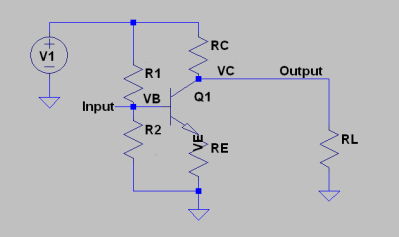 Here is a basic common emitter amplifier, with no capacitors yet. The transistor would like to amplify the base current by its beta to create the collector current. We are going to make a lot of assumptions to make the design process easier and one of those is that the base current is going to be small enough that the emitter current will be the same as the collector current. This means we can think of the collector and emitter currents being simply a beta multiple of the base current.
There are a few problems, though. First, beta is a terrible design parameter. It varies a lot, for a lot of reasons. So we’d like to change our design so that it doesn’t rely so much on beta. In addition, the transistor has to be in its active mode to make this work. For our purposes, this means the voltage on the base has to be able to be about 0.7 V higher than the voltage on the emitter. Since the emitter connects to ground here, you can’t put, say, 0.3 V on the base and expect the emitter to somehow make up the other 0.4 V. However, you can put, say, 3 V on the base and then the emitter will have around 2.3 V — the exact number depends on temperature and the current levels, but we are going to assume 0.7 V is close enough.
The idea behind R1 and R2 is to set the base voltage to turn the transistor into its active region. The input will cause it to wiggle around that number creating variations in the emitter voltage. Those wiggles will create corresponding negative wiggles in the collector side which will be much larger — if we set all the components up correctly. Sometimes, the output comes from the collector. Sometimes, the collector resistor is the load. For our purpose, it won’t really matter.
Close Enough is Usually Good Enough
There is a temptation to try to model exactly what the voltage drop is and what values of resistors you want. But the reality is, the transistors vary quite a bit. Your resistors have a range of possible values. You are not likely to get (or need) something that is exactly perfect. If you need extremely precise circuitry, that’s a whole design discipline on its own.
There are at least two starting points for biasing an amplifier like this. Obviously, the output signal can only go as low as 0 V and as high as the supply voltage (Vcc). The transistor can’t produce more voltage and will clip anything outside those limits. So to get the maximum possible range of output without distortion, it makes sense we’d like to set the collector voltage to half of the supply voltage.
However, sometimes we want to match a stage’s output impedance to the input of the next stage. In that case, you’ll want to pick a fixed RC value because that’s the amplifier’s output impedance. We’ll come back to that topic, but for now, let’s assume we are setting Vc to 1/2 of the supply voltage. You might want to skim ahead to the topic “In Summary” to get the big picture of the steps we are going to take and then return here for the details.
The Details
The next things you need to select are a realistic collector current, and a target gain. Keep in mind that your maximum signal times the gain has to be inside the 1/2 Vcc limit. So an input signal of +/- 1V will limit your gain to about 7. The collector current will influence the power you can deliver to the next stage. For a simple amplifier, you might pick a number somewhat lower than the transistor’s maximum. For example, if you think the device can do up to 100 mA, you might pick 75 mA.
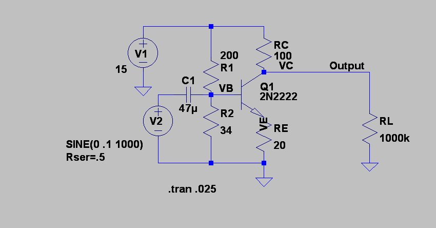
Let’s say our supply voltage is 15 V, Ic=75 mA, and we want a modest gain of 5. We know we want Vc to be 7.5 V which means RC has to drop the remaining 7.5 V. Using Ohm’s law, we can see that RC must equal (15-7.5)/0.075 = 100 ohms. The gain of the amplifier is going to be mostly set by the ratio of RC/RE. So if RC is 100 and the gain is 5 then we solve for 5=100/RE and we can see that RE must be 20 ohms.
We know we need 75 mA through RE and if it is 20 ohms, that tells us that we have Ve = 1.5 V. Since the base has to be 0.7 V above that Vb = 2.2 V. Now we have to select R1 and compute R2. For some of our assumptions to hold true — in particular, that beta (B) won’t affect gain — the combination of R1 and R2 in parallel needs to be much less than RE*(B+1). If we assume B is 100 we get that the resistor combination must be a lot less than 2020 ohms.
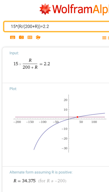 Let’s start with a low value for R1 of 200 ohms. The voltage divider looks simple but you have to account for the fact that R2 will be in parallel with (roughly) RE times beta. However, since we are trying to get much less than that you can probably just ignore that effect. Let’s try it both ways.
By the way, Wolfram Alpha is great for solving these equations if you are too lazy to do it. We need a voltage divider to bring 15 V down to 2.2 V and we know R1 is 200 ohms. Solving you get about 34 ohms.
You could go the long way, though. To make things simple, let’s make up RX=R2*B*RE/(R2+B*RE) — the parallel combination of R2 and RE. Now we can solve for the voltage divider using RX instead of R2 and get the same answer, 34. Now the question is “what value of R2 in parallel with 2000 ohms gives 34 ohms?” Solving for that gives you about 34.6 ohms. So 34 ohms was probably fine. Like I said, close enough is usually good enough when you consider how sloppy we are being with tolerances, temperature variations, and the like.
That’s it! You now know values for all the resistors. You did have to set the supply voltage, the collector current, the gain, and arbitrarily pick one resistor value.
Here’s the simulated circuit with the selected values. Note, there’s a capacitor on the input. We’ll talk about why that capacitor is there in the next Circuit VR.
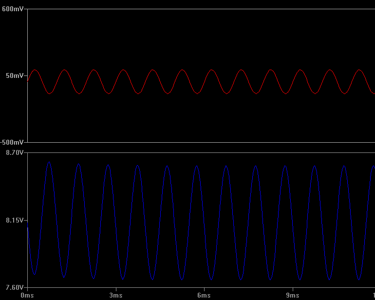
Note the vertical scales are not the same, but they do represent the same amount of voltage delta (1.1 V). For a 0.2 V peak-to-peak input, there is nearly a 1 V output, so the gain of 5 is right, but there is clearly a DC offset. Also, notice that the amplifier inverts. The peaks on the top trace correspond to the troughs in the bottom trace. That’s expected with a common emitter design.
In Summary
Here are the steps for reference:
- Select Vc to be about 1/2 the supply voltage (Vcc)
- Select Ic to be in range of the device (see Update below for more about this)
- Select your realistic target gain (G) (input signal times G has to be less than Vc)
- Compute RC=(Vcc-Vc)/Ic
- Compute RE=RC/G
- Compute Ve=RE*Ic (assuming Ic=Ie)
- Compute Vb=0.7+Ve
- Select R1 (note that R1 in parallel with R2 needs to be much less than RE*(Beta+1))
- Solve Vb=Vcc*(R2/(R2+R1)) for R2
- If you need more precision, solve R2=R2’*Beta*RE/(R2’+Beta*RE) for R2′ and use R2′ as R2
- Verify that R1 in parallel with R2 is much less than RE*(Beta+1)
To ensure that the transistor’s beta doesn’t become significant, you can apply the rule of thumb that RE*(Beta+1) should be much greater than the parallel resistance between R1 and R2. For example, with R1=100 and R2=300 the parallel value is 75 ohms (100*300/(100+300)). But with a 20 ohm RE and a beta value of 100, that leaves you with 75<2020 which is a fair statement.
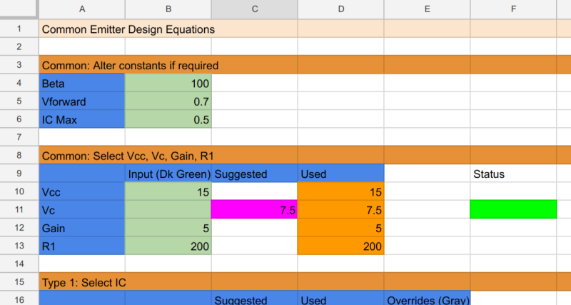
To make things easier, I’ve included a Google spreadsheet that captures all of this. The numbers might change a little because where I will round intermediate results when I’m scribbling at my desk (like the 34 ohm R2), the spreadsheet will not. The instructions for using it are in the spreadsheet.
What About Capacitors?
I promised we’d talk about capacitors, but that’s enough for today. You’ve seen we have a capacitor in the input. This keeps the input from messing up the DC biasing arrangement we’ve created. We’ll add another one, usually, to the output for the same reason. In addition, there’s a third capacitor we can add to promote higher gain without sacrificing DC stability.
Of course, just like with resistors, the trick is finding the values for those capacitors and understanding how they change the circuit. In the meantime, it is easy to experiment with the circuit in the simulator. How does changing RL affect things? By looking at the voltage and current from V2 can you figure out the input impedance of the amplifier? How does changing the amplitude or the frequency from V2 change the output? Can you determine what value of RL gets the most power from the amplifier? Here’s a hint. If Q1 were totally turned off, what value would RL need to be to get the most power? We will touch on many of these topics next time.
Update
One of the great things about Hackaday — and online publishing, in general — is that we can engage in dialog and this post certainly brought up some comments.
Several commenters complained about the high value of Ic. Granted, the Ic value (75 mA) here is higher than necessary for this amplifier. However — as much as I like to round off and estimate — at least one of the comments overestimated the power dissipation.
The selection of Ic — as I mentioned above — may look at several factors and that’s why it is an input into the algorithm. Everything is a trade off depending on what you want to optimize for and in this case I was just pulling out an example with no particular design optimization in mind. However, let’s look at the power for Q1 for a moment.
Calculating Power in Q1
The power in the transistor is like most things related to circuits. The exact number is dependent on a lot of little things that don’t contribute much (like base currents) and one or two major things that tend to dominate. So a close approximation would be the voltage between collector and emitter (Vce or Vc-Ve) times the collector current (Ic). Depending on which datasheet you read and if the case is metal or plastic, you’ll find different values of Pd — the maximum power the device can handle (usually specified at 25C). One datasheet for a metal device says it can handle 500 mW and if you heat sink the case to keep it at 25C, it can handle over a watt. The more common 2N2222A plastic TO92 package, according to ON Semiconductor and Fairchild, can do 625 mW at room temperature, although ST quotes 500 mW.
One comment mentioned that the power through the transistor was 560 mW which is too high for the lowest ratings you find on datasheets without a heatsink. That, however, isn’t the right number because of an oversimplification by the commenter.
Simulated Power
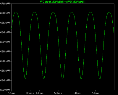
Before I explain further, let’s see what LTSpice says. Here’s a plot of the power through Q1. You can obtain this by pressing Alt while probing the transistor (the cursor changes to a thermometer symbol).
The peak is well under 500 mW at just under 470 mW. True, this is higher than necessary but would work even at the lowest power rating of these devices. You’ll also notice the expression LTSpice used does factor in things like the base current. However, this is with a particular input voltage so the maximum number could be larger, right?
Effect of Input
However, keep in mind the amplifier has a gain of 5 and starts at 7.5V. So the maximum input with a 15V supply is 7.5 divided by 5 or +/-1.5V. That would cause a 7.5V shift in Vc resulting in 0V or 15V out. In reality, you probably can’t actually get to those limits without distortion, but for our purposes, it is reasonable to assume the input is in that range if not less.
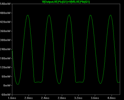
If you put a 1.5V signal in on the simulator, you’ll see the following power in Q1 and you can see the distortion at the low end. You’ll also notice that the power through the transistor is not much higher. In fact, the maximum power — as you’ll see — isn’t at the maximum input anyway.
Why 560 vs 450?
So why the discrepancy? The 560 mW number came from making a simplification. I’m usually all about making a simplification, but this one is a little too simple. It appears that commenters took Vce — the voltage from collector to emiiter as 7.5V and IC as 75mA. The problem is, with no signal input, Vce is not 7.5V. That’s Vc which is the collector voltage with respect to ground.
By design, Ve was 1.5V, so Vce with no signal present is 6V and the power dissipation at that point is 6 times 0.75 or 450 mW. You might think, however, that with the right signal input, Vce will eventually get to 7.5V so the comment is still valid.
But think about what happens when Vc rises. There are two things that happen. First, Ic drops because the voltage across Rc (15-Vc) gets smaller. Second, the input voltage must have gone down by about 1/5 of the amount of the change (the stage inverts with a gain of 5).
If Ic drops and Vce goes slightly up, it will change the power consumed. If Vc drops, that increases Ic. But it also means the base voltage rose, which increases Ve and thus lowers Vce.
So as Vce increases, Ic drops and vice versa. As a result, the maximum power is at the neutral point, which we saw was 450 mW. That doesn’t quite agree with LTSpice, since it is looking at power from the base current, the input signal, and the current through the load resistor, too. If you remove the load and the input from the simulation you get just under 464 mW which is fairly close to our estimate.
Lessons From This
Simulation isn’t always perfect and it is easy to pump 100 amps through a simulated LED if you aren’t careful even though that won’t work well in practice. However, as much as I promote using little shortcuts to make math easier, this is a good example of where it went too far. Sure, in a practical design, you’ll probably want to pick a lower Ic value. But even with a normal 2N2222 this design was within limits at normal temperatures.
So how do you pick Ic? It depends on what you want to optimize for. If you read the datasheets, different transistors will have different sensitivities to the relationship between beta, gain, and noise depending on the collector current. If you are trying to operate at a low power, that may trump everything else anyway.
Other comments noted the low input impedance. That was something I address in the next installment where we will also talk about the capacitors and some other details such as output impedance, as well. However, the best thing there is to match the impedance of the previous stage and since this simulation doesn’t have a previous stage, I didn’t want to spend too much time making a particular match.







I just want to say that you’ve been doing a fantastic job on multiple series that you’ve been posting.
Please keep it up!
On the selection of Ic — for a class A stage like this, the limitation isn’t just the maximum current the transistor can handle, as this is typically of interest when the transistor is used as a switch and operated in either cut-off (fully off) or in saturation (fully on). A usually stricter limitation that applies when it is biassed in the active range, is the maximum power the transistor can handle, P=Vce * Ic. For Vce=7.5V and Ic=75mA, here it will be 560 mW, which is just above the 500 mW absolute max rating seen in the datasheets for the 2N2222. This transistor will definitely run very hot. Usually the Ic for an amplifier like this will be selected based on minimal noise or maximal frequency response, or some compromise thereof. Datasheets sometimes shows typical values, in the 2N2222 datasheet there are some references to 1.0 mA and 20 mA. At 20 mA we will be approaching maximum current gain bandwidth, which might be more desirable. At Vce=7.5V and Ic=20mA, the power dissipation is 150 mW, which is well below absolute maximum.
Good catch. To be honest, I set out to just talk about capacitors in the circuit (next post) and it got so long I decided to go ahead and go deeper. Actually, a 2N2222 with a metal case like we usually use in little ham transmitters has a Pd of 800mW and you can push that with a heat sink. But then again, that’s a class C application. The spreadsheet and algorithm makes you pick Ic and (like you say) there are several reasons you might pick one over the other.
Oh wait, senior moment… 800mA max Ic… bad to get old ;-)
However, Vce is not 7.5V in this case, it is 6V. Granted, with signal Vce will rise, but Ic will then lower, too. If I’m not mistaken, Vce will increase by about 1/5th the rate of Ic decreasing so power in Q1 will always be less than the max (6V x 75mA about) with no signal.
I hate FETs because they’re voltage controlled. With BJT if part of your circuit fails there’s no current and nothing bad happens. FET might stay on and for example cause motor to keep running and injure someone.
No, just no!
This is a badly biased transistor. The choice of the collector current is way too high, and this will lead to many problems:
– the circuit has an input impendance of just 29 ohms (R1//R2)! In the real world, signal sources have an impedance too, and this will create a voltage divider with the circuit’s low imput impedance. With audio sources, for example, the signal will be attenuated by the low input impedance more here than it is amplified by the transistor!
– the transistor has to dissipate 0.45W! This is way too much for a 2N2222, which has a TJA of 200°C/W. In a 25°C ambient, its internal temperature will rise to 25 + 0.45 * 200 = 115°C, reducing its lifetime
– the entire circuit draws more than 1.1W just to amplify a simple signal!
All these problems can be fixed by just reducing the collector current to a more reasonable value, say 5mA.
The theory is correct, but it is clear that this circuit has never been built in practice.
While I do agree that it’s a good idea to teach the basics of electronics to a generation that has started from microcontrollers, we need high quality tutorials, written by people with real world expertise and actually tested, not just simulated. Otherwise those who try this and end up with a non working experiment may get frustrated and think that basic electronics is a kind of black magic that only experts can get right.
Um. VR? Is that what we’re calling simulation now?
To jump on the Ic bandwagon, your step 2 is incomplete. You don’t just pick an Ic that’s within the range of the transistor, you look at the datasheet curves. Most often, there’s an Ic that gives you the highest hFE, and you don’t lose much by going with less current than that. I would ammend this to say, choose the lowest Ic that meets your other circuit requirements.
This is a bad article on so many levels.
Your articles are my favourites, Al. It hurts, so I’m learning. The schematics and visuals are top notch so thank you
what is the difference between a spice simulator and a multisim? can the tutorial on Github be applied in multisim?
“Multisim™ is industry-standard SPICE simulation and circuit design software for analog, digital, and power electronics in education and research.”