
There is one thing that unites almost every computer and logic circuit commonly used in the hardware hacking and experimentation arena. No matter what its age, speed, or internal configuration, electronics speak to the world through logic level I/O. A single conductor which is switched between voltage levels to denote a logic 1 or logic zero. This is an interface standard that has survived the decades from the earliest integrated circuit logic output of the 1960s to the latest microcontroller GPIO in 2018.
The effect of this tried and true arrangement is that we can take a 7400 series I/O port on an 8-bit microcomputer from the 1970s and know with absolute confidence that it will interface without too much drama to a modern single-board computer GPIO. When you think about it, this is rather amazing.
It’s tempting to think then that all logic level outputs are the same, right? And of course they are from a certain viewpoint. Sure, you may need to account for level shifting between for example 5V and 3.3V families but otherwise just plug, and go, right? Of course, the real answer isn’t quite that simple. There are subtle electrical differences between the properties of I/O lines of different logic and microcontroller families. In most cases these will never be a problem at all, but can rear their heads as edge cases which the would-be experimenter needs to know something about.
Consider the Voltage

These differences are best approached from two angles: voltage and current. We’ve dealt with voltage differences before with a look at level shifters, but it’s worth revisiting some of the ground covered there with a short précis as it contains at least one trap for the unwary. We’ve mentioned that there are several different voltage standards for logic, and of those the two that we will most commonly encounter are the afore-mentioned so-called 5V and 3.3V families. In loose terms both recognise a logic 0 as 0V and a logic 1 as 5v or 3.3V, but of course it is a little more complex.
Each individual family of logic has a voltage range instead of a single voltage that it recognises as a particular logic level, and courtesy of TI’s marketing department we’ve reproduced a handy diagram showing them. The trap for the unwary lies with the two different types of 5V logic, the so-called TTL variants accept a much wider range than their CMOS stablemates. Thus a 5V TTL input will detect logic levels from a 3.3V output while the CMOS version will not, and many an engineer including us has been caught by using the wrong chip to interface between levels, only to find a circuit doesn’t work.
The variants carry the labels “TTL” and “CMOS”, but confusingly these refer to their voltage compatibility with the original TTL and CMOS logic families of the 1960s and 1970s rather than their manufacturing. A more recent chip with a CMOS fabrication process will often be available in both a “TTL” and a “CMOS” version. In the popular “HC” CMOS logic series which dates from the 1980s for example the “TTL” versions are denoted by a “T” in the part number such as “74HCT00” as opposed to “74HC00”.
And Then the Current
Once any concerns over voltage have been overcome, we can move on to the current properties. It’s easy to generalise about logic pins as all being the same: low impedance outputs driving high impedance inputs. A typical output should easily be able to supply enough current to drive a reasonable fan-out of other gates, the base of a transistor, or perhaps an LED through a series resistor. And as above in most cases that’s all a designer needs to know. But again therein lie a few gotchas. And since these are of the variety that can result in destruction of the part in question, it’s imperative to explore a little further.
![The daddy of all TTL logic gates, the Texas Instruments 7400 quad NAND gate. Stefan506 [CC-BY-SA-3.0].](https://hackaday.com/wp-content/uploads/2018/07/ti_sn7400n.jpg)
As an aside, the TI Logic Guide is an interesting document from a historical perspective, because unlike almost all other semiconductor product lines we find almost all the major logic families produced since the early 1960s together for comparison, and unbelievably still in production after all these years. We celebrate long-lived ICs such as the NE555 or the μA723, we really ought to do the same for the 7400 quad 2-input NAND gate. First brought to market in 1964 and in continuous production ever since, it is arguably the root from which all our current digital devices and computers grew. Without it we would have certainly reached the same point by a different means, but it could be seen as the first link in the chain of integrated circuits that led to our Core i7s or multicore ARMs today.
Back to our pin currents, and paging through the logic guide we find a significant variation in output currents between families. In most cases they list figures for a run-of-the-mill gate and for a buffer designed with a stronger output, so in this case we’re taking the lower figures from the everyday functions.
Even Hackaday Falls into Pitfalls
It depends of course what you are wishing to do with a logic output, but shall we suggest a stalwart of the breadboard experimenter: lighting an LED? Without a second thought we take a rule of thumb and calculate a series resistor for a 10mA LED current which is fine for an original 7400’s 16mA output, but it comes as a bit of a shock to find the HC series of CMOS chips quoted at 5.2mA. Even in the course of writing this article we’ve found that something we’ve certainly done with a 74HC chip could have been exceeding its rated capabilities without our realising it. We must have lit an LED on a breadboard hundreds of times from 74HC series chips, the fact that we seemingly got away with it likely stems from our not exceeding that other figure for the total current supplied by all pins simultaneously. This experience shows how easy it is to fall into this kind of trap by assuming that all logic outputs are the same, it seems to have been purely by good fortune that we avoided coming face to face with the fact that they are not.
GPIO Is the Front Line of Protecting Today’s More Expensive Chips
So we have arrived at a cautionary tale in our examination of 74 series logic, but of course in a large number of cases we won’t be interfacing with a logic chip in 2018. Instead our logic-level outputs are likely to come through a GPIO pin on a microcontroller or single-board computer. At this point the stakes become significantly higher, as instead of a logic chip costing pennies we have the possibility of damaging something worth a significant price should we overload them. So it is necessary to study data sheets and heed the advise of others carefully indeed to avoid an expensive mistake.
Casting around for information on a few common boards, we find the ATmega328-based Arduino has a comparatively generous allowance of 40 mA per pin, but a slightly confusing 200 mA of total current across the eight pins which share each port register . Meanwhile the ESP8266 with its 3.3V logic has a more modest allowance of 12mA per pin, but with the unexpected bonus that all pins can operate at that current simultaneously.
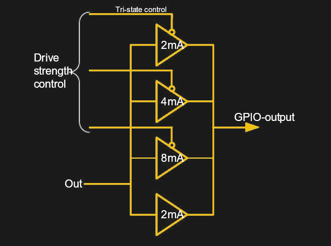
The Raspberry Pi also has 3.3V logic levels, but with an interesting twist. Instead of a single driver behind each GPIO line it has a bank of buffers that can be switched in and out under software control, allowing the output level to be set on a pin-by pin basis. Thus its maximum output can be as high as 16mA, but it can be wound back in applications where a fraction of that drive capability is required.
So we’ve explored the world of logic-level outputs, exposed a pitfall that we’d fallen into, and ended up revealing an unexpected feature of a popular board. It’s still broadly the case that when level shifting is taken care of, all logic lines can talk to each other. But we hope now the chances of your doing so without releasing the magic smoke are decreased.


And when it comes to GPIOs, we might have OpenDrain, OpenSource, asymmetric source/sink, programmable slew-rates and dynamics such as transition-accelerated edges but static high imedance drivers, etc.
Datasheets are nice to have; they should be consulted.
It is always good to go back to the basics these days; specially when newcomers think of GPIO as “connect and go” in detriment of “understand what you are doing first”.I remember when I was first introduced to logic families (about 16 years ago) my fascination and fear of applying the right voltage level to each chip, risking burning down the school if I made a mistake (of course most chips are generally more tolerant that I thought, so that never happed hahaha).
And then there is ECL which gives a new meaning to level shifters.
Yeah, I was a little disappointed that this article didn’t delve into things such as ECL & RTL, or even make mention that the 4000 series can operate with far higher voltages (and hence logic levels) than any “TTL” logic device can deal with.
“But we hope now the chances of your doing so without releasing the magic smoke are decreased.”
Well. Thanks? I guess,
Have we all just had a curse placed on us?
Hang on a minute, I know I’ve got a hex inverter around here somewhere…
With regards to driving LEDs and the 5.2 mA rating of HC chips, two things come to mind:
1. For indicator LEDs, 1 mA is often more than enough.
2. The current rating is going to be limited by how much current can be handled while keeping the output voltage within the limits required (as shown in the graphic earlier in the article). Exceeding the limit will (actually might, due to tolerances, temperature, etc) force the output voltage outside its specification, but the actual power rating (the rating that if exceeded will release the magic smoke) will be higher (max voltage drop for CMOS is 0.56 V, so worst-case power handling at the current rating is 0.56 V x 5.2 mA = 2.9 mW, i.e. tiny – several times that will be OK).
Amazing write up Jenny. I’ve been tinkering with digital logic since I was old enough to learn how to solder. And as it happens also includes old enough to travel by myself and even buy components. By the way Jenny, my entire collection of Series 74 Logic thank you immensely.
The variable drive strength on SOC processors is for controlling edge rates to limit ringing and EMC issues.
Ah, makes sense. I did wonder. Thanks.
But equating current-limiting with slew-rate limiting is making quite a few assumptions about the circuit being driven! I guess those assumptions are valid often enough for it to be a useful practice, and I’m sure it’s cheaper than more exotic approaches.
I’ve seen “slew-rate-limited outputs” quoted in quite a few datasheets, and never dug in to investigate whether they meant current-limited or something more complicated. Do you have a sense, Bob, of how common this approach is versus other approaches?
Actual reason why it works revolves around this differential equation: V=L*dI(t)/dt.
L being parasitic inductance from tracks on the PCB; dI(t)/dt being rate of change of current as a function of time. Signal frequency is not very important, but slew rate is. When you want high frequency signals, the rise time must be fast if you want neat square edges, otherwise you would see some RC charging curve instead of brickwall square wave.
Now assuming your GPIO can drive the signal very fast, dt would be equally small. So for a given output current, the voltage may overshoot fairly high, causing ringing. Ringing is caused by resonance between parasitic inductance and capacitance of the track. If you want to limit this ringing, you must either increase dt or reduce dI. Changing dt is not really possible (at least not cheaply), since your transistors have fixed physical parameters. On the other hand, changing dI is very easy because output stages usually include multiple MOSFETs to get large current capacity. This drive strength trick only consists in changing the amount of MOSFETs driven at once. So this feature is mostly “free” for IC designers.
Another way to solve ringing is by adding a series resistor. This will both increase total output impedance and reduce channel bandwidth due to parasitic capacitance of the track. If you think about it, paralleling multiple MOSFET for higher drive strength is like pulling up/down the output with multiple resistors in parallel (MOSFET Rds(on)): this gives higher output current and lower output impedance.
Uh
In cases like this you should consider lubrication requirements as well
Speaking of magic smoke…
I have noticed several FPGA dev boards now include Arduino headers. Looking at schematics of one [Arty] I see the 5V line is present – and no obvious level shifting.
Keeping in mind that FPGA’s can run at 3.3, 2.4, 1.8 or even 1.2V at the core – what happens when you plug in an older 5V Arduino shield?
The only arduino I have uses 3.3V logic. You should verify the specs of both boards before mating them.
74LVT is useful. 3.3v out, but 5v tolerant on inputs.
3.3V out and 5v tolerant in is the best. Learned the hard way not all logic components support this…
Great write-up, and this is very useful to know.
The reason why your 74HC chips didn’t let out the smoke when being asked to deliver 10mA, exceeding the 5.2 mA in the specs — is that 5.2 mA is the maximum it can deliver while keeping the output voltage within the minimal VOH to maximum VOL, so that any subsequent connected input will see sufficiently high and low levels. As long as you don’t exceed the absolute maximum current rating for the output, your device will survive. For the 74HC00 for example, this limiting value for output current is 25 mA, so anything below this will not be fatal. And modern LEDs light up nicely at 5 mA…
BAHAHAHAHAHAHAHAHAHAHA!!!!!11!!!!!!!1!!!!!!!!!!!11!!!!!11111
I LOLed.