
If your introduction to digital electronics came more years ago than you’d care to mention, the chances are you did so with 5V TTL logic. Above 2V but usually pretty close to 5V is a logic 1, below 0.8V is a logic 0. If you were a keen reader of electronic text books you might have read about different voltage levels tolerated by 4000 series CMOS gates, but the chances are even with them you’d have still used the familiar 5 volts.
This happy state of never encountering anything but 5V logic as a hobbyist has not persisted. In recent decades the demands of higher speed and lower power have given us successive families of lower voltage devices, and we will now commonly also encounter 3.3V or even sometimes lower voltage devices. When these different families need to coexist as for example when interfacing to the current crop of microcontroller boards, care has to be taken to avoid damage to your silicon. Some means of managing the transition between voltages is required, so we’re going to take a look at the world of level shifters, the circuits we use when interfacing these different voltage logic families.
Do You Even Need A Level Shifter?
It might seem odd to start a treatise on level shifting this way, but the first question for the designer when looking at making a 3.3V part talk to a 5V part should be this: Do I even need a level shifter?
If the 3.3V part is an output and the 5V one an input, the lower voltage part can hardly damage the higher voltage one with overvoltage. And you are not likely to encounter a logic input that might demand so much current that it would damage your output (If you do, use a buffer!). If you are lucky the logic voltage ranges of the two devices may even coincide. For example 3.3V TTL logic shares the 0.8V and 2V thresholds for logic 0 and logic 1 transitions with 5V TTL logic, so a 3.3V TTL output can drive a 5V TTL input without any extra hardware required.
In the other direction, driving a 3.3V input from a 5V output you might expect that a level shifting circuit would be required, and in many cases you would be right. But before reaching for that shifter it’s worth taking a look at the detailed specifications of your 3.3V input. Many devices are designed to be 5V tolerant, and you might be lucky enough to find that your circuit could use one and avoid the extra circuitry. For example the 74LVC series contains a range of 5V tolerant 3.3V versions of many 74-series ICs.
CMOS And TTL: A Level Shifting Cautionary Tale
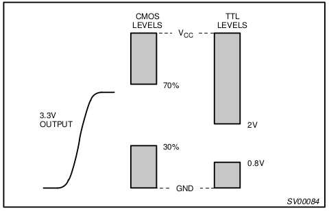
When directly driving logic you’d normally use at 5V from a 3.3V output there is one cautionary tale of which to take heed, a personal confession of an electronic failure. CMOS logic defines its logic thresholds as a percentage of supply voltage, which with a 5V supply puts the logic 1 threshold of 70% well above the 3.3V logic 1. Some CMOS ICs such as the 74HC4053 analogue switch I used in a Raspberry Pi project don’t quite follow this standard and will work from a 3.3V TTL output, so I was lulled into a false sense of security and reached for another 74HC part to connect to my Raspberry Pi with a new design. As you might expect it failed to work, and of course I wasted time looking everywhere else but my defective choice of part. If there is a moral to this story it is to always read the datasheet carefully, and use the TTL-compatible parts such as in this case 74HCT, when they are available.
If your 3.3V device inputs are not 5V tolerant and your 5V inputs lack 3.3V compatible thresholds then sadly you won’t be able to interface them across voltage levels without a shifter circuit. There are many choices available to you including a whole host of dedicated level shifter devices such as these ones from TI, but aside from personal preference some of them will be dictated by your application. Will it be a step-up, a step-down, or do you need a bi-directional level shifter? If you decide not to use a dedicated part or a 5V tolerant gate in your design, here are a few of the many alternatives.
Step-down level shifters
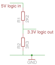
The simplest possible step-down circuit is a resistive divider. Drive your 5V output into a chain of resistors, from which you tap your 3.3V logic input. A chain consisting of a 2.2k and a 3.3k resistor should produce a 3V output from an applied 5V input. It does not preserve the fan-out characteristic of the 3.3V output and you need to be aware of any capacitances that may also reside in whatever logic is connected to it and the effect they may have along with the resistors on fast rise times, but it should suffice for most simple level downshifting tasks facing a hobbyist. There are variations on this circuit that use diodes instead of a resistor to achieve the required voltage drop.
If the divider is not suitable for your application and you still eschew a dedicated shifter, take a look further down the page at bidirectional shifters.
Step-up level shifters
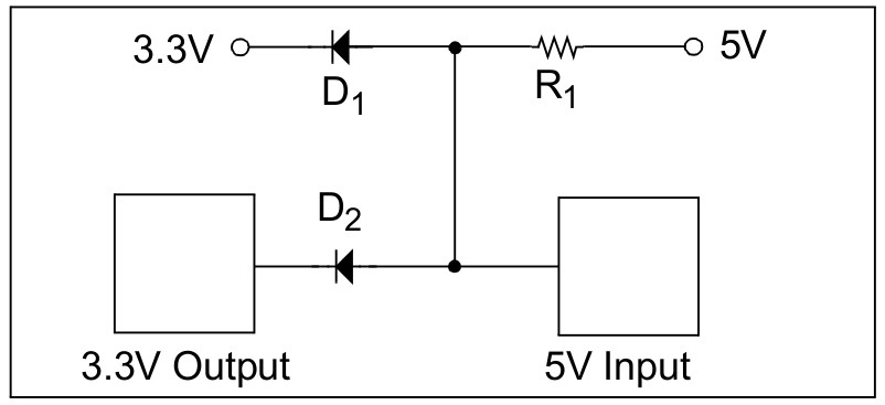
For stepping up from 3.3V logic to 5V logic and assuming you are not safely within the TTL thresholds as described above such that you can do without a shifter, you will require something a little more complex than the resistive divider in the previous section. The simplest circuit uses a pair of diodes with careful biasing and choice of series resistor as shown in the diagram to the right. The application note it comes from advises that the resistor should be significantly less than the input impedance of the 5V gate, to avoid its being part of a resistive divider with that impedance having an effect on the output voltage.
A rather more obvious circuit uses a MOSFET or bipolar transistor as a switch, driving the gate or base with the 3.3V logic and taking the 5V logic output from the drain or collector. This is very similar to using a gate with an open-collector output in the same application. This is a simple and reliable circuit, but it must be borne in mind that it inverts the 3.3V logic level.
Bi-directional level shifters
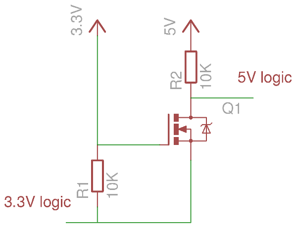
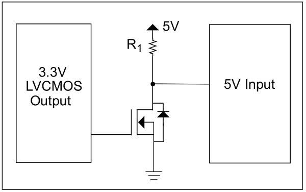
The circuits in the previous two sections are both only suitable for unidirectional logic lines, but not in the case of a bidirectional bus. As before there are plenty of off-the-shelf bus level shifters from a range of semiconductor manufacturers to choose from, but if these are not suitable for your design then a handy alternative can be made with a MOSFET and a couple of resistors. It’s also worth pointing out that this doesn’t have to be used on a bidirectional bus, it can serve as a general purpose level shifter for the cost of a 2N7000 or similar, indeed this is a personal favourite for this application. You can readily buy this circuit on a breakout board from several electronics suppliers if building it yourself doesn’t appeal. For more information on its operation take a read of the Philips application note AN97055 (PDF), which examines its use on an I2C bus. (Edit 2025: The old link went dead. Fortunately, the folks at Adafruit have a copy of AN97055.)
It can be a worry, when you first have to ensure that different logic levels are safely interfaced. Will my 5V Arduino harm this 3.3V sensor? We hope that after reading this piece you’ll have some more confidence, and we’ve equipped you with enough to make some sense of the topic. We’ve not covered every possible technique, but if you read some of the attached application notes and then search the web for real-world usage they should fill in any gaps.


I like using Schmitt triggers (usually in inverters) for 3.3V->5V translation, at least when there are many I/O lines. A single chip with no other parts can handle 6+ lines easily. The accepted minimum high-voltage of the 5V input is usually well within the minimum output of a 3.3V part.
That is rather marginal, if you consider worst case tolerances. I prefer to use HCT parts, e.g. HCT08 (AND gate) or 74HCT244 or 74HCT245.
Needed to interface my BBB (3V3) and took some 74LS240’s (Datecode 8549) out of a 20 years old partsbin. Works like a charm to beef up the BB’s outputs (Machinekit) to buffer to the opto inputs of steppermotors (DQ543MA).
To add something short to a tedious long story. Lots of combinations are possible. Some work beautifully, some don’t so always check voltage levels when interafacing between different technolologies (Even if they are powerd from the same supply).
I have standardized on the TXS0104E for level shifting – with 4 level shifters in one package, it lets me interface 3.3V SPI devices to 5V buses without any hassle. I use a MCP1702-3302 as a 3.3V regulator as well.
SPI has no bidirectional pins, so voltage dividers for MOSI, CLK and SS/CS and nothing for MISO is entirely sufficient. Keep It Simple, Sir.
My thoughts exactly.
Hello,
I have an SPI communicatin betwwen a 3.3V sensor and a 5V PIC18, I understand that I need a voltage dividers for the 3 lines MOSI, CLK and SS, I want to know if I need a pull-up or a pulldown on MISO, CC Line ?
4-wire SPI has no bidirectional pins. 3-wire does. There’s a TON of parts that only do 3-pin.
Voltage dividers limit how fast you can run SPI. High resistance values may help limit the current the divider consumes, but they increase the rise and fall time, which in turn lowers the maximum rate at which you can transfer data. Lower values unnecessarily consume more current and contribute towards your device’s total power dissipation. “Sufficient” is subjective to what the design requirements are, not some universal maxim.
‘Nothing’ on MISO in many cases means frying that pin when interfacing 5V parts with a 3.3V uC.
Interesting. But I don’t think these work if the parts not 5v tolerant? Probably worth mentioning this. Is there another simple way that works with non-5v tolerant parts? (I don’t think the ESP32 / ESP8266 are 5v tolerant).
Did you even read the article?
I believe that I saw somewhere that ESP8266 is 5V tolerant as long as you power it from 3,3V source.
From my test results, it is better to power the ESP8266 from a little more than 3V3 to be really rock solid and 5V tolerant. I experienced some shoot-through failures when powered from 3V3 in 5V environment – probably the 3V3 supply was not hard enough and fluctuated down a bit upon transmitting. 3v6 regulator saved the project, no more burnt GPIOs.
5 years too late here, but I think you just misunderstood what the author means here. The data output of the ESP is 3.3V, which isn’t enough, so we have that go into a level shifter circuit to “boost” the signal. At no point does the ESP itself get affected by anything other than 3.3V, the 5V comes after it, not before it. :)
For some circuits, it is enough just ensuring not enough current to damage the input.
For this I have often used an inline 100 or 200 ohm resistor when interfacing a 5V output to a 3.3V input.
The factor here is that the 3.3v device has diode clamping on the inputs. If it has you can safely just use a resistor to limit the current. If it doesn’t have diode clamping on the inputs then you are taking a risk.
Yes, but 100 or 200 Ohm gives a very high current, I would increase the resistor
just be careful that you have enough load on the 3.3V
In the picture “A diode logic level step-up circuit. From Microchip app note DS41285A (PDF).”, what is the function of D1?
I’ve read the datasheet but that doesn’t make it more clear.
I think it creates an alternative current path, so that the current from +5V through R1 doesn’t need to flow through your 3.3V Output (and it’s maybe none existed output protection diodes).
ah thanks for that.
It prevents the voltage at the anode (‘hot’) side of D1 to never exceed 3.3V + VD1.
Therefore the output of the 3.3V component at all times will not exceed 3.3V + VD1 – VD2 = 3.3V.
If you read the datasheet closely you will see that this diode, D1, makes the high voltage 4.0v in the case where the 3.3v output is a ttl part that has a high output of around 2.4v. Took me a while too!
I believe it prevents feeding (+5V – D2 diode drop) > 3.3V into the 3.3V output. D1 ensures that the 3.3V output sees at most (3.3V + D1 diode drop – D2 diode drop) = 3.3V. Meanwhile the 5V input sees (3.3V + D1 diode drop) when the 3.3V output is high which is less than 5V but greater than Vih_min.
thanks
If you closely at the datasheet D1 is actually for the case where the 3.3v part is TTL (having a high level of 2.4v). In this case D1 will pull the input level to the 5v part to around 4.0V. Took me a while too!
The way I think of it is that current flows from the 5V supply through R1 and D1 to the 3.3V supply, which causes the usual 0.7V drop across D1. This is added to the 3.3V supply, creating a voltage around 4V at the junction of D1 and R1. This is high enough to be a logic high to the 5V device. And the 3.3V device can still pull down to around 1V, which is low enough for the 5V device to see as a low.
@mime. My best reasoning about D1: If you removed D1, when the 3.3V output is low, it is connected across D2 to a 3.3V voltage source which will drive the output to 3.3V – ~0.6V (diode drop). The 5V supply has a current limiting resistor (R1) to deal with that problem on its leg.
Interestingly, this circuit seems to require the 3.3V output to act as a current sink. If it were a high-Z output (effectively an open circuit), D2 wouldn’t “turn on” and the 5V input would just float high all the time.
Regarding the homebrew level shifters, it needs to be reiterated that they won’t work well past a certain (low) signal frequency. I have had mixed results with driving WS2812b leds for example.
WS2812b’s are finicky and high frequency bastards compared to anything else ‘entry level’ hobbyists dabble with.
The ‘mosfet and two resistors’ style level shifter should work if you reduce the values of the resistors (4k7 instead of 10k I guess), but then the sink and source current output of the microcontroller/SoC is increased, maybe even beyond specifications.
Alternative is using a high-speed buffer ic.
I’ve had alot of success underdriving ws2812’s at 4.2v instead of 5v. My raspberry pi zero happily drives a matrix of them without any level conversion, with a perfectly acceptable drop in max brightness, no burned retinas, obvious gains in battery longevity, no fuss no muss.
Prior to that I did use a small Mosfet level converter, works well with the ws2812.
i drive my ws2812b strands directly from a 3.3v esp-12 with a separate 5v for the power source Never had any problems.
Ditto this for me. No obvious issues.
Just as a tip for usinging the MOSFET bidirectional shifter, ensure the transistor’s Vgs max threshold is 2.5V or less (3.3v-0.7v). The Philips AN suggests parts with th of 2V or less, to ensure a good margin. Going to a lower voltage e.g.1.8v would require an even lower threshold of 1.1v.
If your introduction to digital electronics came more years ago than you’d care to mention, the chances are you did so with 5V TTL logic.
Guilty! In fact, I always thought all these mentions of “3.3v” were just about sneaking by with a lower-power “1” signal.
One other way to interface 3.3V with 5V CMOS, which is admittedly mildly dicey, is if you have control over the power supplies. A number of 5V chips can run as low as 4.5V, and 70% of 4.5V is 3.15V. Conversely, many 3.3V devices can run as high as 3.6V. So by goosing the 3.3V supply a little and dropping the 5V supply a little, you can sometimes get them to play a little nicer and still be in spec. I wouldn’t recommend using 3.6V and 4.5V unless you’ve got really precise control over the supplies — maybe targeting 3.5V and 4.8V to have some leeway would be best (since some 5V parts only go down to 4.75V).
Note that I’m not recommending this in general, but if you have free reign over all of the supplies in the system, and they’re adjustable, and you’re trying to save a few pennies… it could work.
I seen the suggestion of raising the 3v3 supply to 3v6 in at least one official manufacturer application note. If you have a poke around your favorite parts supplier you will find that extremely precise 3v6 LDO’s are common now as well.
Some tips –
I like making retro computers so level shifting is often an issue.
CMOS (Complementary Metal Oxide Substrate) is a fabrication technology and that technology does not specifically dictate input or output voltage levels. However there are *common standards. The trap is that some CMOS chips are specifically made to work with TTL voltage levels. So it is best to use terms like TTL LVTTL LVC etc.
Carefully chosen current limiting series resistors can be used between a TTL (5v) output and a non-5v tolerant 3v3 input if the 3v3 device has diode clamping on the I/O pins and will accept input voltages 0v6 above Vcc (most do).
The noise margin between a LVTTL 3v3 device driving a TTL 5v device is very small. Fortunately you can buy very accurate voltage regulators (Linear LDO’s) that are precisely 3v6 output. Most 3v3 chips are speced to run between 3v0 and 3v6 so by running them at 3v6 you will lift the noise margin and hopefully have reliable operation for parts that normally don’t play nicely.
When stuck – remember three diodes will drop 1v8
Even 5v tolerant chips are getting hard to find with things like FPGA and CPLD but some make excellent level shifters while still doing the glue logic function.
A humble transistor with a base series resistor and a collector load (pull up) resistor will shift up from 3v3 to 5v but the logic is inverted – just fix it in software.
Another great article from [Jenny List], thank you!
I’m off to read the linked notes. It’s always good to learn new things.
Dear Hackaday, please compliment your resident artist. This article’s picture reminded me of another great technical genre artist, Robert Tinney who used to do those fabulous BYTE magazine covers. That I even made this comparison then made me realise how germane your artist’s perception of the topic at hand is. And thank you too Jenny, both of you keep up the good work!
+1
+2
We love Joe’s work! It’s tremendously satisfying to put in a ton of work on a long-form piece and then it gets some sweet art on the top. He makes us look so good.
Oh and BTW: a few months ago, by popular request, we started using the original-resolution versions of the banner art in the banner. Right-click (or whatever) and enjoy!
This goes well with articles on FPGA’s. Of course, the next step is to follow up with an article on 2.4V, 1.8V etc.
By the time you reach 1.2V logic things can get hairy.
For about a buck USD: Low Cost Bi-Directional Level Shift Module Characterization (TE291)
http://www.whiskeytangohotel.com/2016/12/low-cost-bi-directional-level-shift.html
Another bidirectional level shifter, but with bipolar transistors: http://www.hagtech.com/pdf/iic.pdf
also shown in this page https://playground.arduino.cc/Main/I2CBi-directionalLevelShifter
This topic has relevance to the world of retro gaming; some are claiming that reproduction cartridges from China are using 3.3v chips when the original cart would have used 5v chips. They are then going on to claim that this could cause damage to the console itself if level shifting is not done properly.
To me, though, it would seem that if anything would be damaged, it would be the cart with the 3.3v chips on it, not the console with 5v chips. Any thoughts here? Any way to tell by looking if a board has been wired with proper level shifting for a 3.3v chip interfacing with a 5v console?
For switching up, what’s wrong with a 2222 NPN resistor with 5V on C, 3.3v signal with 100kohm to ground on B, and the 5V requiring gizmo on E?
This won’t work.
I see your thinking but an NPN transistor needs a voltage 0.6v (approx) higher on the base than emitter to conduct.
This would result in about 2.6v on the emitter.
Hi, the link for the Microchip Tips and tricks is broken. I found the original link from microchip:
http://ww1.microchip.com/downloads/en/DeviceDoc/chapter%208.pdf
Thanks for updating this old (but still useful and high-ranking in searches) article :-)
I actually know nothing about electronics, but I’m learning. What I’d like to know is how to convert a whole (simple) circuit designed to run at 5v to 3.3v.
I’m following schematics to clone a SBC from WDC, the company that still produces the 65xx family of chips. They designed their SBCs to work with USB ports, at 5V. But I want to convert the SBC to 3.3v.
What changes should I make to the components to make them 3.3v compliant?
I’m not asking someone to give me the right new values for resistors and capacitors, but how to calculate these new values.
Thanks.
Eschew? Are you sure you were reaching for THAT word here?
The “A simple resistive downshifter” picture is a bit incorrect. There should be 5V logic OUT and 3.3V login IN.