
Everybody wants to give FPGA development a try and here’s a great way to get into it. You can build your own Persistence of Vision display using a $30 dev board. It’s a fun project, and you’ll learn quite a bit about designing for an FPGA, as well as using the Quartus design software.
The inspiration for this article comes from [vpecanins] who did an example project where you wave the board back and forth and a message appears in mid air. This uses the MAX1000, a pretty powerful yet odd FPGA board for about $30. It contains an Intel MAX10 (when did Intel start making FPGAs? Remember, Intel bought Alterra back in 2015). I find the board odd because it also holds an accelerometer that you can talk to using SPI. That’s a little strange for a generic FPGA board, but paired with eight on-board LEDs it’s perfect for this demo.
Since I didn’t find any written documentation for this example, I thought we’d help out and take you on a step-by-step tour of the project. What’s more, in a future installment, I’ll show you how to make some significant changes to the tutorial that will make it even more practical as a base for other projects.
 Just for motivation, have a look at the video below to see what the project does. I modified the text (WD5GNR is my call sign), of course. The effect is better in real life, but the video will give you the idea. The FPGA monitors the accelerometer reverses the order for flashing the LEDs on and off to form the characters. It is a pretty impressive demo since it takes advantage of the unique features of the board, is non-trivial, and isn’t too much Verilog to swallow if you are just getting started.
Prerequisites
To start with, you’ll need to install Quartus. The Lite edition is free and very capable. You can download the files and open the test0.qpf file in the demo02_led_text directory. You may get a nasty dialog about replacing the database if you have a newer version of Quartus than the original files used. You can safely agree to that.
File Tour
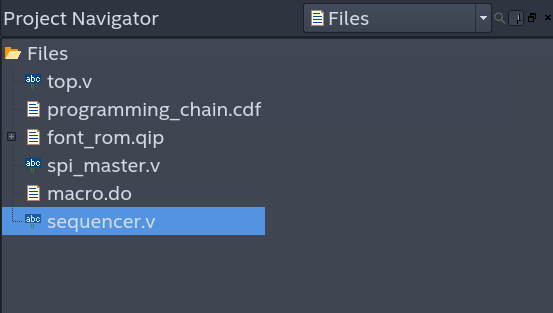 On the project navigator inside Quartus, you can select Files and you’ll see the project has only a few:
- top.v – The main Verilog code.
- programming_chain.cdf – This file should tell Quartus how to program the configuration into the chip, but it is missing. That’s not a problem though. It isn’t really necessary and it is easy to recreate.
- font_rom.qip – A component that uses Altera IP (Intellectual Property) to create a ROM with the character patterns in it.
- spi_master.v – Code for talking to the accelerometer.
- macro.do – This file doesn’t actually exist and is apparently left over from the author’s earlier efforts.
- sequencer.v – Code for using the accelerometer.
 If you expand the font_rom.qip componet in the list, you’ll see there is a Verilog file hidden there. That file was generated by an IP wizard, so while you can look at it, you shouldn’t need to touch it. It uses the Altera Sync RAM IP block to create a chunk of memory. One thing to note is that the Verilog file does specify an init file which is font5x7.hex. That’s a standard hex file with the contents of the ROM. By the way, this is a ROM in name only. It is implemented in RAM but there’s no interface to write to it so from the design’s point of view it is read-only. It is not, however, nonvolatile. It will get rewritten every time you reconfigure the FPGA.
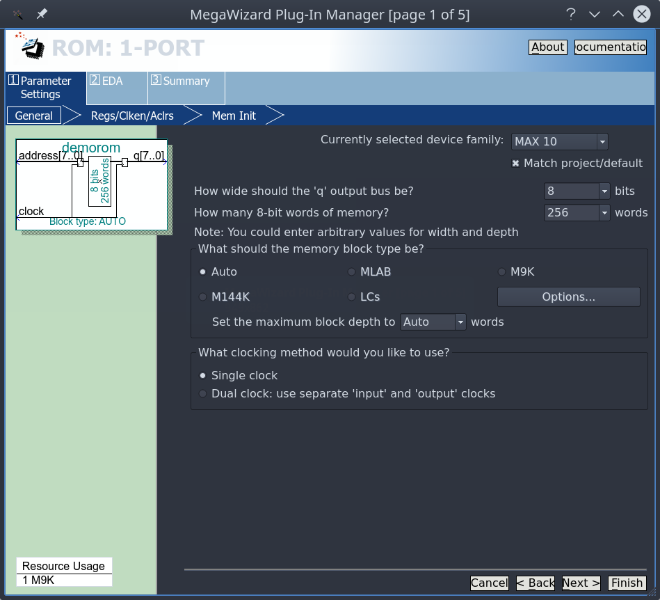
Again, all of that was set up by answering some questions in an IP wizard. You should be able to open the IP to change it with the Parameter Editor, but there seems to be some file missing to allow that or, perhaps, the author set it up by hand. However, you can see the process if you go to the IP Catalog in Quartus and open up Library | Basic Functions | On Chip Memory | ROM: 1 Port. It would be easy to replace the existing ROM with your own if you wanted the practice.
The Top Module
The top module has an interface to the 12 MHz system clock, the user button (which it uses as a reset), and the 8 LEDs. It also contains the signals to talk to the SPI accelerometer and 8 bits of parallel I/O that appears to be used for debugging (the design just copies some internal signals to those pins).
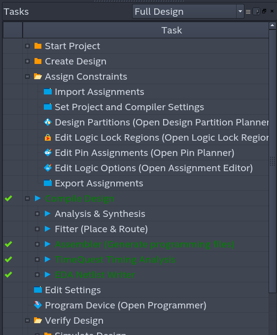 To tell the software where those ports need to go, you need to set location constraints, which the author already did. There are many ways you could do this. However, one way is to locate the tasks section of Quartus and pick “Full Design.” Then you’ll see a folder for “Assign Constraints.” Open that up and pick Edit Pin Assignments. From there you can set up all the I/O pins for the top module — their names, the type of pin it is, and exactly which pin on the FPGA it maps to.
If you prefer, you can use the Assignments item on the main menu and pick Assignment Editor. I like that better as it is like an easy-to-read spreadsheet format. If you didn’t already have the starter project, how would you know which pins the LEDs and things are on? That data is in the technical reference manual for the board. There’s also a spreadsheet in the directory that documents the assignments.
The rest of the module creates the SPI component and the sequencer component. If you notice, the sequencer has a single output “direction” which is mapped to the dir signal in the module. The other connections are just housekeeping like a clock and a connection to the SPI component.
What Do the Blocks Do?
There are a series of always blocks in the rest of the file. These generally correspond to a block of logic and, when combined with the posedge or negedge keywords, usually define a flip flop circuit.
always @(posedge CLK12M or negedge nrst) begin
	if (!nrst) begin
		divider <= 32'b0;
		divider_out <= 1'b0;
	end else begin
		if (divider != div_coef) begin
			divider <= divider + 1;
			divider_out <= 1'b0;
		end else begin
			divider <= 32'b0;
			divider_out <= 1'b1;
		end
	end
end
The first one simply divides the clock down since 12 MHz is a little fast. You can adjust the speed by changing the value of div_coef near the top of the file. The second block handles the ROM addressing. Each character is 5 consecutive bytes out of the ROM. So the addr_lsb counts from 0 to 4 and then rolls over, setting char_inc to 1 as a signal to go to the next character.
always @(posedge CLK12M or negedge nrst) begin
	if (!nrst) begin
		addr_lsb <= 3'b0;
		char_inc <= 1'b0;
	end else begin
		if (divider_out) begin
			if (addr_lsb == 3'b101) begin
				addr_lsb <= 3'b0;
				char_inc <= 1'b1;
			end else begin
				addr_lsb <= addr_lsb+1;
				char_inc <= 1'b0;
			end
		end else begin
			char_inc <= 1'b0;
		end
	end
end
Another always block handles the character address. There are 16 characters stored in the foo array. The pos variable starts at zero and increments when char_inc is set. It rolls over at 16. This is good defensive programming because you might change the 16 number to something else. However, the 4 bit counter would roll over at 16 anyway, so in this case, it is a bit superfluous and I wouldn’t be surprised if the tools optimize that logic out anyway.
always @(posedge CLK12M or negedge nrst) begin
	if (!nrst) begin
		addr <= 10'b0;
	end else begin
		if (dir) begin
			addr <= {foo[4'b1111 - pos] - 'h20, 3'b101 - addr_lsb};
		end else begin
			addr <= {foo[pos] - 'h20, addr_lsb};
		end
	end
end
The foo array is where you can change the message. It really isn’t an array in the strictest sense. It is just some assignments that are indexed. That means at the moment you can’t change the message without rebuilding the FPGA, but we will fix that in the next installment. The real heart of everything, though, is the following always block. It forms an address where the top bits are the current character minus 20 hex. That subtraction cuts off non-printable characters. The bottom bits are the 3 bits counting from 0 to 4. That means the first location in the ROM is a space and takes up the first 5 words. Then the rest are the ASCII characters in order, each taking their own 5 words.
However, the address has an odd property. If the dir bit is set from the accelerometer, the character that provides the top bits is “flipped” end-to-end by subtracting the index into foo from 1111 binary. The bottom bits are also flipped by subtracting them from 5. This makes the foo index go 15, 14, 13… instead of 0, 1, 2… and also makes the line count go backwards.
So if dir is 0, the message is played back left to right and if dir is 1, it plays in reverse. The rest of the file is simple. The code instantiates the ROM and assigns its outputs to the various LEDs.
And the Rest…
I’ll let you explore the spi_master.v and sequencer.v files on your own. I will point out, though, that the sequencer is a good example of a state machine. There are 11 states, and the circuit moves from one to the next to send and receive the data it needs from the accelerometer. So, for example, here’s the code for the first three states:
case (state)

// 1. Read WHO_AM_I register (Addr 0x0F)
STATE_Whoami: begin
state <= STATE_Whoami_Wait;

spi_request <= 1'b1;
spi_nbits <= 6'd15;
spi_mosi_data <= 31'b10001111_00000000;
end

STATE_Whoami_Wait: begin
if (spi_ready) begin
state <= STATE_Init;
led_out <= spi_miso_data[7:0];
end
spi_request <= 1'b0;
end

// 2. Write ODR in CTRL_REG1 (Addr 0x20)
STATE_Init: begin
state <= STATE_Init_Wait;

spi_request <= 1'b1;
spi_nbits <= 6'd15;
spi_mosi_data <= 31'b00100000_01110111;
end
Note that led_out is for debugging and in the final code, that output isn’t connected to anything. The general structure of each state is to either do some action and set the next state or wait for some action to occur and then set the next state. Pretty easy. Of course, more complex state machines might have to decide which state is next, but not in this case. The real work is in the STATE_Compare state:
			// 6. Compare X_OUT of the accelerometer to know the swipe direction
			// The acceleration is maximum at the edges of the swipe, detect that
			// and change direction accordingly.
			STATE_Compare: begin
				state <= STATE_Read;

				if (saved_acc < -8'Sb0010_0000) begin
					led_out <= 8'b1110_0000;
					direction <= 1'b0; end else if (saved_acc >  8'Sb0010_0000) begin
					led_out <= 8'b0000_0111;
					direction <= 1'b1;
				end else begin
					led_out <= 8'b0001_1000;
				end
			end
		endcase
Don’t forget that led_out isn’t used in the actual project — it was just for debugging. When the sign of the acceleration changes beyond a dead band, the direction bit changes. Simple.
Configuration
You know you want to change the message to say something else so go ahead and modify the code where it sets up foo. Double clicking the compile design task will generate a SOF and POF file. The SOF file will send the configuration to the board but won’t save it. If you reset or power cycle you’ll lose that configuration on the board. You must program the POF file for the board to dutifully reload the configuration on start up.
If you double click the Program Device entry in the task list you’ll get a separate window for the programmer. You can follow the instructions in the MAX1000 user’s guide for the exact details, but the idea is to associate the SOF or POF file with the FPGA on the JTAG chain. If you see the device in the programmer, that’s good but if not you can always Auto Detect. Just make sure you have the hardware set for Arrow-USB-Blaster and the mode set to JTAG. You also may need drivers for your particular set up, so take a look at the user’s guide.
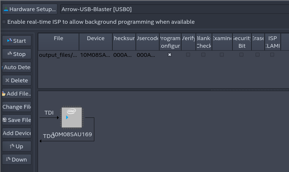
The only tricky part is when you program a POF file you need to be sure the Program Configuration check box is ticked. Then press Start and you are on your way.
Wrap Up
Learning FPGAs can be daunting. After all, you need to learn a complex piece of software, plus you need to learn Verilog (or VHDL) and get used to a new way of thinking about solving problems. On top of that, there are the usual things you have to learn about anything like how the devices connect and how to download a “program” to the board. But playing around with known working examples like this is a great way to gain an intuitive sense of how everything works.
With so much to learn, the [vpecanins] tutorial might not be your first step. But it wouldn’t be a bad second step. You can check out our FPGA boot camp if you want a gentler introduction. The first 3 boot camps are hardware agnostic, so what you learn would apply to the MAX1000. Intel has a lot of training available to learn about Quartus. In fact, there’s so much training it is sometimes hard to know where to start.
Next time, I’ll show you how to add a UART to the project so you can change the display on the fly through the USB port. That sounds hard but I’ll use a few tricks to make it relatively easy. If you want to try something easy, consider changing the code to use the LEDs like a bargraph to show the acceleration it reads.


Here in Poland you need a permission from govt to own and use FPGAs as they are considered ‘important parts of a weapon’. Guess I’ll stick to 8-bit AVRs :(
Can you link to info on the relevant law? I can’t find any mention of this on Google.
tme.eu (which is based in Poland) seems quite happy selling FPGAs without any permissions asked.
I’ve bought FPGA dev boards from a Polish retailer (Kamami). I couldn’t tell you if they shipped them from Poland or it only applies to Poles but I think you need to check into that.
“A full installation of the Intel FPGA Complete Design Suite v18.0 requires approximately 14GB”
How can that be possible?!
It’s nice to notice that Intel haven’t forgotten Linux.
Check also the RAM-usage, I am impressed by this bloatware.
https://www.intel.com/content/www/us/en/programmable/support/support-resources/support-centers/licensing.html
” Many Intel® FPGA software tools and intellectual property (IP) cores require a license file to operate. (…) In your license file, you will see two dates: the maintenance expiration date and the license expiration date. The license expiration date controls the length of time a product can be used . The license stops working when it reaches the expiration date. ”
Yes, license® is a serious topic one should be careful of, be very careful, it’s easy to get burn®.
No wonder why it’s missing documents®, DIY-peoples seems to have other options.
When I read through code like this instead of learning something I just go away angry at people that write code with lines like “end else begin.”
Looks like wd5gnr.com hasn’t been updated in a long time.
No it has not…
What “Devices” need installed with Quartus Lite (on the download page it is asking me)… the choices are: Arria, Cyclone, Stratix… none of which come up as keywords in the MAX10 datasheet
Nevermind, somehow I re-clicked the dropdown menus and saw MAX10 in the device list.
Wrote this little tool to dump the font5x7.hex file and print the chars to screen:
https://gist.github.com/nmz787/6a9681d93fd67e4b58ffb5caab257b82
Well the rendering of the link I pasted was certainly not expected, sorry for the long output!