Right now, we’ve got artistic PCBs, we’ve got #badgelife, and we have reverse-mounted LEDs that shine through the fiberglass substrate. All of this is great for PCBs that are functional works of art. Artists, though, need to keep pushing boundaries and the next step is obviously a PCB that doesn’t look like it has any components at all. We’re not quite there yet, but [Stephan] sent in a project that’s the closest we’ve seen yet. It’s a PCB where all the components are contained within the board itself. A 2D PCB, if you will.
[Stephen]’s project is somewhat simple as far as a #badgelife project goes. It’s a Christmas ornament, powered by two coin cells, hosting an ATTiny25 and blinking two dozen LEDs via Charlieplexing. The PCB was made in KiCAD, with some help from Inkscape and Gimp. So far, so good.
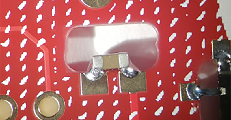
The trick is mounting all the components in this project so they don’t poke out above the surface of the board. This is done by milling a rectangular hole where every part should go and adding castellated pads to one side of the hole. The parts are then soldered in one at a time against these castellated pads, so the thickness of the completed, populated board is just the thickness of the PCB.
The parts used in this project are standard jellybean parts, but there are a few ways to improve the implementation of this project. The LEDs are standard 0805s, but side-emitting LEDs do exist. If you’d like to take this idea further, it could be possible to create a sandwich of PCBs, with the middle layer full of holes for components. These layers of PCBs can then be soldered or epoxied together to make a PCB that actually does something, but doesn’t look like it does. This technique is done in extremely high-end PCBs, but it’s expensive as all get out.
Still, this is a great example of what can be done with standard PCB processes and boards ordered from a random fab house. It also makes for a great Christmas ornament and pushes the boundaries of what can be done with PCB art.


Nice. I’ve wondered about mounting devices in a pcb like this before, but hadn’t considered castellation!
Something that is not mentioned in the article, but worth pointing out, is the stock diodes shine light at the opposite milled wall, lighting up the PCD. If you go an look at the GIF, this results in a really nice halo effect! I don’t know about anyone else, but I really like it, especially as a Christmas ornament.
Someone’s project taking advantage of just that https://hackaday.io/project/28155-silly-pcb-designs/log/71025-embedded-leds-work/
Very nice, a bit of a polish on the edge and a couple of these would make some cheap jumbo 7-segments!
I am working on a 100mm 7 segment RGB clock at the moment, using that technique:
https://hackaday.io/project/20142-rgb-seven-segment-display-rssd/log/155852-new-design-includes-special-ws2813-footprint
My WS2813 footprint is not what you would call castellated, but it’s a cutout with solderpads on the bottom PCB side. Close enough!
2D PCB? I’m sure you mean 3D.
No, they mean 2D. The components don’t stick out.
I see your point (components in the depth of the layer) but… at the end you have a FLAT board.
I was initially thinking the same thing as Sir JMD, though I did come to the same conclusion as ilcilcali.
So, I suppose calling it 2D is silly. It’s only going to be half the thickness, at least, of the same board using normal surface mounting. Hardly more “2D” than normal.
I guess it’s “2D” if you picture each side of the PCB existing on a plane coinciding with the respective surface of the PCB. Kind of like how a sheet of paper approximates a 2D plane, even though it does have a non-zero thickness in reality.
0603 part is 1.6×0.8mm. 1.6 coincides with standard FR4 thickness. So they can be inserted vertically. Making such pads can be a problem though because cads kind of assume that a through hole pad spans across all layers. But I’m sure there are ways around that. Basically you need 2 matching circular pads, but not plated and 2 layers connected to different pins.
Noo, that’s my idea! I’m designing a PCB that does that right now!
If your circuit contains entirely diodes, resistors and caps, you may have hit upon the most easy-to-solder SMD design imaginable. Just pop the part into the hole and solder, no need for part-holding.
But then you get solder surface tension pulling/sucking the parts up, you’d have to tape one side first
Please share the results with us! Seriously, I’m really curious of the final outcome.
I’m not pretending that I invented this ;) I heard about this about 10 years ago on an internet forum, but somehow I never really tried it myself. Looking forward to seeing your results!
It’s like the sadistic sequel to cordwood construction!
I love it! I hope I never have to work on it!
Exactly! Cordwood was my inspiration to do this.
a different meaning to the term “thru hole”
Not all CAD programs assume that. Look for ‘buried vias’.
It’s a lot of manual work.
I remember seeing a PCB business card on here years ago doing the same thing.
This is almost it https://hackaday.com/2010/05/25/mass-storage-business-card/, but mounting chips this way is decades old
I’ve got at least one computer mouse that does it that way. Weird how the chip in there is not only a microcontroller–it also has an orifice on the bottom which exposes the little camera used to pick up light from an LED and track motion. Of course the camera is on the underside of the IC, so it’s mounted in a hole cut from the PCB. Thought it was pretty clever for such a simple, mundane device.
Its super common, especially in LCD matrix controllers in the 80s; to keep the pin orientations the same on opposing halves they “flipped” the chip by mounting it in a hole
No way, this is exactly what I was working on. Somehow other people always seem to beat me to an article.
That’s because you spend too much time reading HaD and not enough time making. No, this doesn’t apply to anyone I know intimately, no, it does not.
You may or may not be on to something there. But a genius in my own mind I certainly am.
Ewww!
Yes Rodney we know you are talking about yourself. And you had to use the word intimately! Not an image any of us wanted, thanks a lot!
He knows himself in the biblical sense.
Slightly OT, but a while back someone posted a link to a nice table that listed the most efficient way to control a given # of LEDs vs number of available pins, comparing a lot of methods like shift registers, charlieplexing, and even “use a bigger microcontroller”. Haven’t been able to find it, anyone got a link?
Aaaargh! I know the one you’re talking about, it was like a spreadsheet, right?
I’ve just spent several minutes searching and can’t find it. This is the closest I’ve come but I don’t think this is the one you’re thinking of: https://hackaday.com/2013/04/08/another-way-to-look-at-charlieplexing/
Close, but Maave found it (see below). Thanks though!
Here’s the chart
https://hackaday.com/2018/09/30/whats-the-cheapest-way-to-scan-lots-of-buttons/
This article might interest you as well
https://hackaday.com/2018/06/14/general-purpose-i-o-how-to-get-more/
Thanks, that’s it!
“the next step is obviously a PCB that doesn’t look like it has any components at all”
Ugh!
Ok Brian, are you sure you really want to go there? Do you really want to propagate THAT idea?
Think of it this way…
When someone does it at home it’s “an artist pushing the boundaries”.
When manufacturers do it it’s “an evil corporation making sure we can’t hack our own stuff so that we will fill up the landfills and buy more”.
See the problem yet?
Meh, the extra manufacturing cost and space requirements of this technique should be enough to make most manufacturers say “No, thanks”.
There is a way to make it repairable (several actually). I worked on doing just this in the late 1980’s. It’s remarkably simple once you have the intuitive leap. Our (completed, populated) board costs were on the order of $50-100k each, so it was very worthwhile to make them repairable. I’ll wager very few are in landfills. :)
The company decided to keep it as a trade secret rather than patent it after we spent all the time writing up the patent applications. No idea if they ever exposed it.
Additionally there are a number of other logical extensions you can use the technology for, and ways you can make it more reliable.
You made PCBs which didn’t look like they had any components at all? In the 1980s? And they were repairable? Note that i was replying to what Brian wrote about the “next” step, not what is actually in the article.
Also, I’m not talking about the manufacturer doing reworks. I’m talking about the home diyer hacking their toys. Is not the first step to look at the board, see what parts are on it, maybe look at some datasheets, poke at some pins, etc… If the PCB looks like it has no components… that becomes quite a trick!
One last thing, are those ways of making it repairable something to do at home or part of the design process done by the manufacturer. How many manufacturers today are trying to make their goods more repairable or hackable? i think most see that as zero gain to them at best, an actual loss to future sales at worst.
This process looks like it makes assembly a pain which is probably why it is expensive to do at scale (or time-intensive to do one-off).
I mean I’m sure somebody could figure out a way to reliably automate it with a pick-n-place machine and a reflow oven. If they really wanted to. This was done by hand, but it probably doesn’t have to be.
Maybe this is what you are thinking of. It is for inputs – not LEDs, but some of the methods might still apply.
http://www.openmusiclabs.com/learning/digital/input-matrix-scanning/index.html
Well, this was supposed to be a reply to CE’s comment. I’m not sure why it’ appeared as a new comment.
Been rolling that way for almost 5 years now. https://hackaday.com/2014/03/01/the-credit-card-sized-gameboy/ There are a few comments on this page pointing out other uses of this method.
Warning: Nomenclature overload. Flat-pack is already a thing. http://www.ti.com/packaging/docs/searchtipackages.tsp?packageName=CFP
dont forget Flatpak software