
The concept of negative resistance has always fascinated me. Of course, a true negative resistance is not possible, and what is meant is a negative differential resistance (NDR). But of course knowing the correct term doesn’t do anything to demystify the topic. Negative resistance sounds like an unusual effect, but it turns out to be relatively common, showing up in places like neon lamps and a number of semiconductor structures. Now’s as good a time as any to dig in and learn more about this common principle.
NDR means a portion of a device’s I/V curve where the current falls with increasing applied voltage. The best-known semiconductor device exhibiting negative resistance is the tunnel diode, also known as the Esaki diode after one of the Nobel-Prize-winning discoverers of the quantum tunneling effect responsible for its operation. These diodes can perform at tremendous speeds; the fastest oscilloscope designs relied on them for many years. As the transistor and other technologies improved, however, these diodes were sidelined for many applications, and new-production models aren’t widely available — a sad state for would-be NDR hackers. But, all hope is not lost.
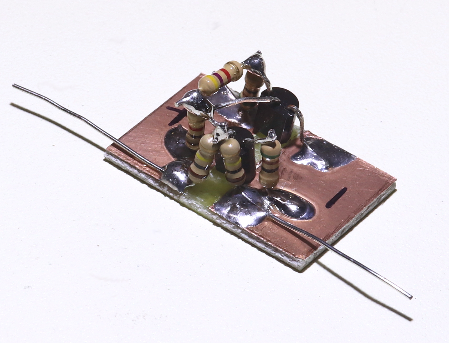
Rummaging through some old notebooks, I rediscovered an NDR design I came up with in 2002 using two common NPN transistors and a handful of resistors; many readers will already have the components necessary to experiment with similar circuits. In this article, we’ll have a look at what you can do with junkbox-class parts, and in a future article we’ll explore the topic with some real tunnel diodes.
So, let’s see what you can do with a couple of jellybean transistors!
Faking It
Tunnel diodes are relatively rare beasts – although these days, like most things, you can find them on eBay – so I wanted to come up with a circuit that allowed experiments with negative resistance using common parts. While there are a number of DIY solutions to NDR devices, they were all a little “fiddly” for my tastes. For instance, you can make your own NDR components by heating galvanized sheet metal (just don’t breathe the fumes!), or use the NDR region in a reverse-biased transistor emitter-collector junction to make an extremely simple LED flasher, but it’s difficult to control the parameters of these devices.
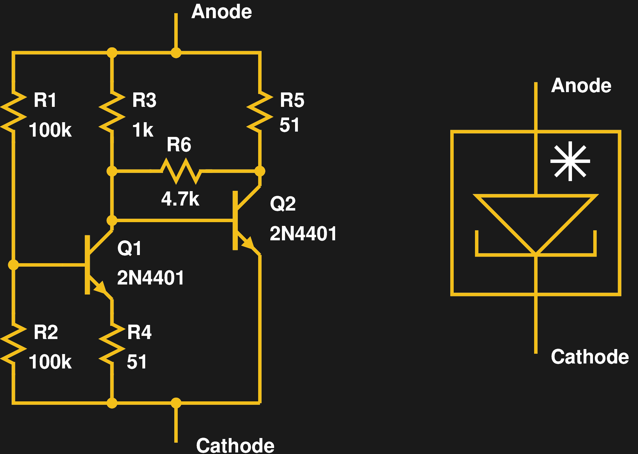
With this in mind, back in 2002, I came up with a two-transistor circuit where the negative resistance region is somewhat controlled by selection of resistors. The circuit emulates a two-terminal device like a tunnel diode, and for the purposes of this article, I made a shorthand symbol for it that resembles a tunnel diode inside a box. An asterisk inside the box reminds the reader that this isn’t an actual diode.
Referring to the schematic, Q1 acts as an inverter, with its collector initially rising with the supply, but subsequently falling as it is biased on with increasing voltage. Q2, configured as an emitter follower, dumps current across the device’s terminals at lower voltages, but relents as the supply increases. The result is a circuit whose current increases with applied voltage up until a point, but then decreases relatively linearly for a while — the negative resistance region — before increasing again. R6 is a key part of this circuit; it affects the width and linearity of the NDR section of the curve. The circuit is still a little “fiddly,” but at least you have some knobs to turn.
Although I initially tried both 2N3904 and 2N2222 transistors in this circuit, I found that 2N4401’s work best, probably because their gain is a weaker function of collector current than the other two types. This is what electrical engineers would call a “bad” circuit, since it depends on individual transistor characteristics: you can’t count on getting the same results from a number of different transistors with a typical manufacturing spread of parameters. So, don’t use this in any real designs; it’s just for fun.
In any, case, if you find that some experimentation is in order, changing R6 is a good starting point; smaller values stretch the NDR region wider. LTspice simulations work well for this circuit — at least qualitatively. Due to its dependence on transistor parameters, the results you see on the bench may vary from simulation quite a bit, but I found the simulation can be used to gain intuition about the behavior and inform experiments on the real thing. Actually, this pretty much sums up most of my experience with electronic simulation.
The original prototype from 2002 was assembled on a small piece of perfboard, while I chose some copper clad and ugly construction for the most recent version. Either way will work fine; this circuit is only suited for low-speed operation where construction techniques aren’t terribly important.
I subsequently discovered that Chua, et al. had published a 1985 paper describing a wide variety of such circuits made from either BJTs or MOSFETs. Unfortunately the article is paywalled — the DOI is 10.1109/TCS.1985.1085599. If you’re interested in designing circuits like this, that paper looks like a goldmine of information — but it’s not worth $14.
Tracing Curves
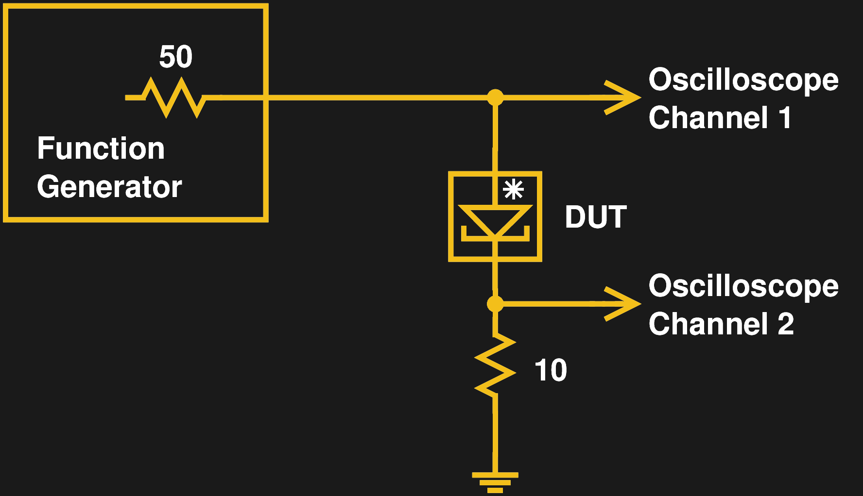
Ideally, you’d use a curve tracer to investigate a circuit like this, but I don’t own an actual curve tracer [scribbles on to-do list]. In 2002, I collected curves point-by-point with a pair of DMMs — this works, but consumes a lot of your day. This time around, I hacked together a curve tracer with a function generator and an oscilloscope. As shown in the figure, a 10-Ohm resistor is used as a shunt to detect the device current on channel 2 of the scope, while channel 1 measures the voltage across the device-under-test and the sense resistor. The function generator outputs a ramp waveform — even a sine will do in a pinch — at around 100 Hz.
With the oscilloscope in X-Y mode, you can get an indication of the I/V curve of the device. Of course, there’s an error introduced because channel 1 is measuring the voltage across the DUT and the resistor; the voltage across the DUT is actually the difference between the channels. Unfortunately, the scope I was using doesn’t let you use math traces in X-Y mode (I’m looking at you, Rigol). If you wanted to generate accurate I/V curves with this setup, the easiest way might be to capture the trace data, then generate the curves in your favorite plotting package.
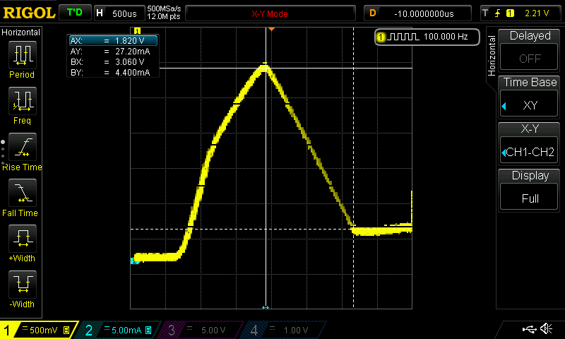
For just a few points, however, it’s easy enough to do the math by hand. That’s how I calculated the value of the negative resistance in the NDR region shown in the trace. Based on the two points shown with the cursors, the region has an average differential resistance of -64 Ohms. As you can see from the plot, the region is a decently linear from around 1.55 V to 3.0 V of applied voltage, passing between 27.2 mA and 4.4 mA over that span. After that, the current ramps back up.
Depending on the specific transistors used, the I/V curve may show a pronounced hysteresis loop where the thresholds for the NDR region depend on the direction of the voltage sweep. In this case, the device is exhibiting memory or stateful behavior. This property of NDR devices has been used in digital circuitry.
LC Oscillator
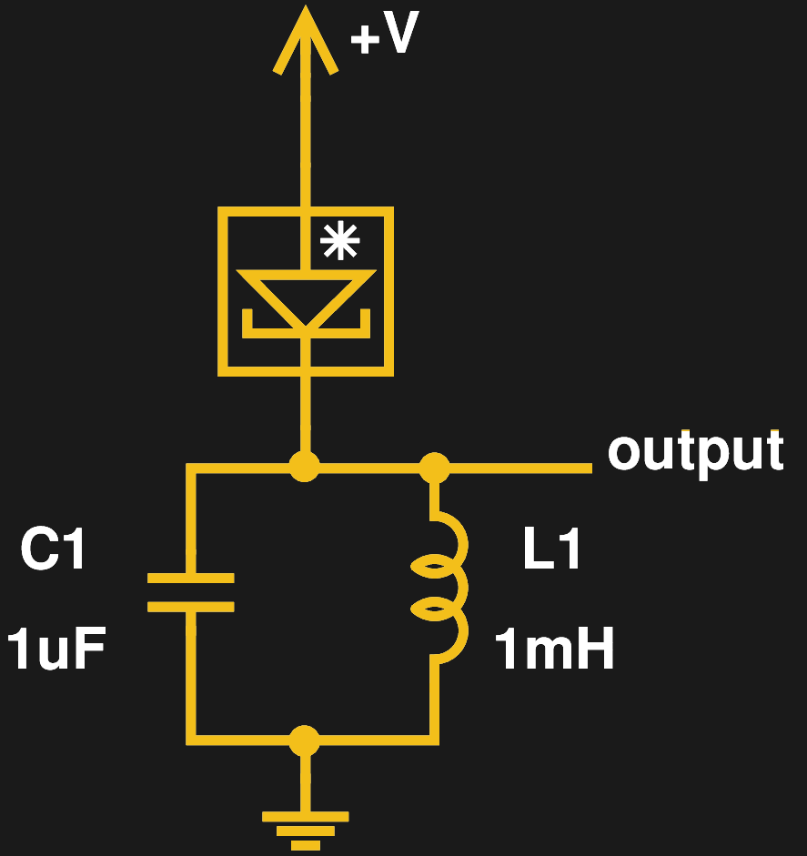
What can you do with a negative resistance like this? One of the classic uses for an NDR device is in oscillators. Consider a simple parallel LC tank circuit. Normally, any resistance across the tank (or even that in the inductor or capacitor themselves) is enough to damp any initial oscillation to zero over time. Supplying current through a negative resistance, however, will have just the opposite effect, causing the oscillations to build and continue indefinitely. Of course, there is no free lunch; we have to use a power supply to bias the NDR device into the negative resistance region.
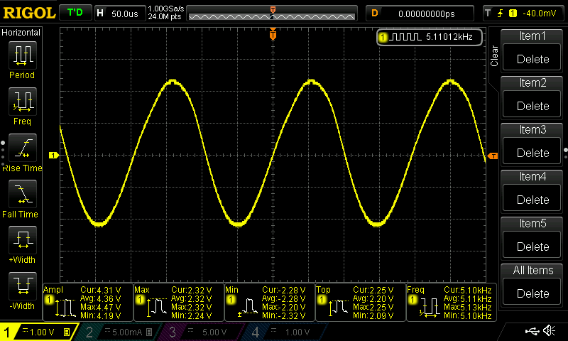
Shown in the schematic is a 5 kHz oscillator I made this way using a 1 uF capacitor and a 1 mH inductor. For zero-tolerance parts — which I did not happen to have in stock — this should result in a 5.033 kHz oscillation. The measured frequency was 5.11 kHz. I found that the circuit oscillated for supplies between 1.6 V and 3.6 V, with the best waveform around 3.5 V, although it didn’t self-start above 2.6 V. The output amplitude is around 4.3 V using a 3.5 V supply.
Keen eyes might notice a component missing in the simple schematic. For audio-frequency oscillators like this one, it might be OK to have the return current flow back through the power supply if the leads are short. For anything faster, you should certainly add a bypass capacitor or two across the supply as close as possible to the circuit.
This simple circuit isn’t suited for oscillators much above audio frequencies, unlike actual tunnel diodes, some of which can reach into the GHz range.
Amplifier
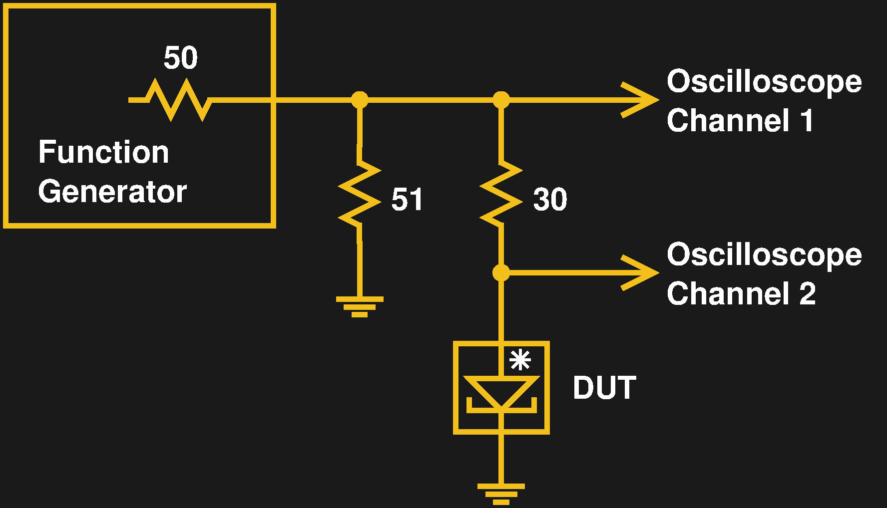
It’s also possible to use NDR devices as amplifiers. In the classic tunnel diode amplifier circuit a resistor is used to bias the diode and set the gain. With a two-terminal amplifier circuit, multiplexing the input and output can be tricky. Probably the best way is to AC-couple the signals, but I chose to stay close to the canonical circuit using the offset control of the signal generator to adjust the DC bias on the diode.
A second problem is that the gain of such an amplifier depends on the magnitude of the external resistor relative to the negative resistance value. With a 50-Ohm signal generator and a -64 Ohm device, there’s not much room to choose the external resistor. To make measurement a bit easier, I added a 51 Ohm resistor across the output of the signal generator, making the output impedance around 25 Ohms. This allows adding a 30 Ohm gain-setting resistor without blowing our budget of 64 Ohms.

The input signal to this amplifier is at the top of the 30 Ohm resistor, while the output is taken at the bottom. The resulting amplifier is very non-linear, so it’s best used for square waves where such distortions aren’t an issue. By adjusting the signal generator offset, I was able to find a bias point around which the device showed some voltage amplification. In the oscilloscope image, you can see that the output signal (cyan trace) has a higher amplitude (1.84 V) than the input signal at 1.26 V. The 30 Ohm resistor and the NDR work like the familiar resistive divider, except they increase the input voltage!
Tunnel Diodes
My next adventure with NDR will take a look at some vintage Russian 3И306M gallium arsenide tunnel diodes I bought on eBay a few years ago. If we’re lucky, I’ll also find some of the germanium tunnel diodes I had at one point. In the mean time, you can dig out some transistors and have some fun at the bench, or check out another of our articles on negative resistance.


Tunnel diodes were also used to generate ~0.5V steps into 50ohm loads. Risetime was 10s of picoseconds, so well into the GHz region!
Nowadays I’d use a comparator with LVDS outputs.
CML-output comparators are also good, unless you need a larger voltage swing or current output, in which case laser diode drivers intended for optical networking seem to be the best bet, at least from what I’ve found.
The Borg: Resistance is futile, you’ll be assimilated!
The Author: Negative resistance is fun, you’ll be amazed!
Very interesting article, thank you!
:o)
“Q2, configured as an emitter follower”
It is not an emitter follower but a commun emittter.
This is a good video showing a bit more about tunnel diodes by Alan Wolke:
https://www.youtube.com/watch?v=PuG8CCUbg58
These are fascinating (and very old!) components but very fiddly to use.
Actually the Tunnel Diodes that GE were making are still around. Point your browser to search for the 1N3712 and you’d be surprised. I also have two. Then they were not cheap.
But do they still work? Tunnel diodes were infamous for failing with time because of the high doping required to make them function.
Both of mine still do.
You can also search for GaAs gunn diodes they have the same U I curve
Also useful: some early LEDs had a slight negative differential resistance region around 1.66V Vf specifically the green ones used in certain camera flash units though it was often the case that they would vary too much for production use due to ambient temperature changes.
Think the reason was that they were slightly different being based on Zn rather than Ga or In, and these also had a pronounced colour shift from green to orange depending on current from 0.3 to 9mA.
Possibly related?
If you want to read a scientific article mentioned in the text, just enter its DOI number on the Sci-Hub search page. The DOI is 10.1109/TCS.1985.1085599 .