Sometimes, rather than going the commercialistic route, it can be nice to make a gift for that personal touch. [Mahesh Venkitachalam] had been down this very road before, often stumbling over that common hurdle of getting in too deep and missing the deadline of the occasion entirely. Not eager to repeat the mistake, help was enlisted early, and the iCE bling earrings were born.
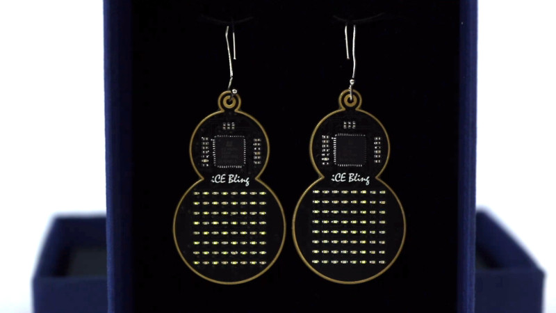
The earrings were a gift for [Mahesh]’s wife, and were made in collaboration with friends who helped out with the design. The earrings use a Lattice iCE40UP5k FPGA to control an 8×8 grid of SMD LEDs. This is all achieved without the use of shift registers, with the LEDs all being driven directly from GPIO pins. This led to several challenges, such as routing all the connections and delivering enough current to the LEDs. The final PCB is a 4-layer design, which made it much easier to get all the lines routed effectively. A buffer is used to avoid damaging the FPGA by running too many LEDs at once.
It’s a tidy build, which makes smart choices about component placement and PCB design to produce an attractive end result. LEDs naturally lend themselves to jewelry applications, and we’ve seen some great designs over the years. Video after the break.


Cool, but would my wife wear them?
Umm, why are you asking us?
What is the use of them? Any special purpose it is used to satisfy?
If she wears hoop earings she will wear these… What am i talking about, i want to pierce my ears just to use them lol
Cool! Happy to see electronut making blingy stuff!
Link is dead due to what appears to be a website redesign, but the project is still up, now at this link:
https://electronut.in/ice-bling-fpga-beautiful-led-earrings-with-lattice-ice40/
Thanks, link fixed.